首页 > 集成电路 IC > STM32F103C8T6

STM32F103C8T6


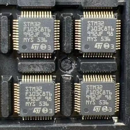
ARM Cortex-M3 MCU 频率为 72 MHz,具有 64 KB 闪存、20 KB SRAM、USB、CAN 和电机控制外设,适用于主流嵌入式应用。.

0

有效库存
转到查询

Image for reference only

制造商零件:

STM32F103C8T6

包装:

LQFP-48(7 x 7 x 1.4 毫米)

品牌:
您可能感兴趣的其他建议.
说明

"(《世界人权宣言》) STM32F103C8T6 by STMicroelectronics is a mainstream ARM Cortex-M3 microcontroller running at 72 MHz with 1.25 DMIPS/MHz, featuring 64 KB Flash and 20 KB SRAM. It integrates two 12-bit ADCs (1 MSPS, 10 channels each), four timers (one motor-control PWM with dead-time), and communication interfaces including 2x I2C, 3x USART, 2x SPI, 1x CAN 2.0B, and 1x USB 2.0 full-speed device. A 7-channel DMA controller offloads data transfers from the CPU.

Packaged in LQFP-48 (7 x 7 x 1.4 mm) with 37 GPIOs (most 5V-tolerant), the MCU operates from 2.0V to 3.6V across -40 to +85C with Sleep/Stop/Standby low-power modes and VBAT backup. SWD and JTAG debug supported. ECOPACK2, RoHS compliant, halogen-free. ECCN 3A991.a.2. Active. Widely used in motor drives, IoT end nodes, USB peripherals, and industrial control. Pin-compatible clones available from GigaDevice (GD32) and WCH (CH32).

The STM32F103C8T6 is a mainstream-performance ARM Cortex-M3 32-bit RISC microcontroller manufactured by STMicroelectronics, operating at up to 72 MHz with 1.25 DMIPS/MHz performance. The device features 64 KB Flash memory and 20 KB SRAM, making it one of the most widely used entry-level ARM MCUs in the STM32 portfolio.

The MCU integrates two 12-bit ADCs (1 MSPS, up to 10 channels each), three 16-bit general-purpose timers, one 16-bit motor-control PWM timer with dead-time generation, two watchdog timers (independent and window), and a 7-channel DMA controller. Communication interfaces include two I2C (SMBus/PMBus), three USARTs (ISO 7816, LIN, IrDA), two SPIs (18 Mbit/s), one CAN 2.0B Active, and one USB 2.0 full-speed device interface.

The device operates from 2.0V to 3.6V with Sleep, Stop, and Standby low-power modes. A VBAT pin supports RTC and backup register retention. The internal clock system includes an 8 MHz factory-trimmed HSI RC (1% accuracy at 25C), a 40 kHz LSI RC, and support for 4-16 MHz HSE crystal and 32.768 kHz LSE crystal for RTC.

Packaged in a 48-pin LQFP (7 x 7 x 1.4 mm) with 37 GPIOs (most 5V-tolerant), the device supports SWD and JTAG debug interfaces. A 96-bit unique device ID provides individual chip identification. The STM32F103C8T6 is ECOPACK2 compliant, RoHS compliant, and halogen-free. ECCN: 3A991.a.2. Product status: Active. Available in tray packaging (standard 1500 pcs/tray for LQFP48).

The STM32F103C8T6 operates as a mainstream embedded microcontroller with the following subsystem architecture:

1. Cortex-M3 Core: The 32-bit ARM Cortex-M3 CPU executes at up to 72 MHz, featuring 3-stage pipeline, single-cycle multiplication, hardware division, and 1.25 DMIPS/MHz performance. NVIC (Nested Vectored Interrupt Controller) supports up to 43 maskable interrupt channels with 16 priority levels. The core supports Sleep, Deep-Sleep, and Standby low-power entry via WFI/WFE instructions.

2. Memory Subsystem: 64 KB Flash with prefetch buffer and ART-like acceleration for 0-wait-state execution at 72 MHz (for LQFP48 medium-density devices). 20 KB SRAM is accessible in a single cycle. A 7-channel DMA controller handles peripheral-to-memory and memory-to-memory transfers without CPU intervention.

3. Clock System: Multi-clock source system: HSE (4-16 MHz external crystal), HSI (8 MHz internal RC, 1% accuracy), LSE (32.768 kHz for RTC), LSI (40 kHz for IWDG). A PLL multiplies the clock source to generate the 72 MHz system clock. Clock security system (CSS) detects HSE failure and auto-switches to HSI.

4. Analog Subsystem: Two independent 12-bit successive-approximation ADCs with up to 10 external channels each (ADC1 has additional internal channels for temperature sensor and VREFINT). Maximum sampling rate is 1 MSPS at 14 MHz ADC clock. Dual sample-and-hold capability enables simultaneous sampling.

5. Timer Subsystem: One advanced-control timer (TIM1) for motor control PWM with complementary outputs and dead-time insertion. Three general-purpose 16-bit timers (TIM2-TIM4) for input capture, output compare, PWM generation, and encoder interface. Two basic timers (TIM6-TIM7) for DAC triggering and timebase. SysTick for OS tick generation.

6. Communication Subsystem: All peripherals connected via APB1 (36 MHz max) and APB2 (72 MHz max) buses. USART1 on APB2 (high-speed), USART2/3 on APB1. SPI1 on APB2, SPI2 on APB1. I2C1/2 on APB1. CAN and USB on APB1. Pin multiplexing allows flexible peripheral-to-pin assignment.

别针组 计数 类型 说明
GPIO (PA-PD) 37 输入/输出 General-purpose I/O, most 5V-tolerant, with alternate function mapping for USART, SPI, I2C, TIM, CAN, USB, ADC
VDD 4 P Digital power supply (2.0-3.6V)
VSS 4 G 数字地面
VDDA / VSSA 2 P/G Analog power and ground for ADC/DAC
VBAT 1 P Battery backup for RTC and backup registers
NRST 1 I System reset (active low, internal pull-up)
BOOT0 1 I Boot mode selection (main Flash / system memory / SRAM)
OSC_IN / OSC_OUT 2 输入/输出 HSE oscillator pins (4-16 MHz crystal)
OSC32_IN / OSC32_OUT 2 输入/输出 LSE oscillator pins (32.768 kHz for RTC)
应用 说明
Motor Drives Advanced PWM timer with dead-time and encoder input for BLDC/stepper motor control in drones, robots, and CNC machines
IoT End Nodes Low-power modes and multi-protocol interfaces (I2C, SPI, USART, CAN) for sensor hubs, smart meters, and wireless module hosts
USB Peripherals Built-in USB 2.0 full-speed device interface for HID, CDC, and custom USB class devices without external USB transceiver
工业控制 CAN bus for industrial networking, ADC for sensor acquisition, and PLC/inverter control in factory automation
消费电子产品 Cost-effective MCU for gaming peripherals, GPS platforms, medical handhelds, alarm systems, and HVAC controllers
模型 制造商 兼容性 主要区别
STM32F103CBT6 ST 兄弟姐妹系列 Same package (LQFP-48), 128 KB Flash (2x), same RAM and peripherals
STM32F103RCT6 ST 系列升级 256 KB Flash, 48 KB SRAM, LQFP-64 with more GPIOs and ADC channels
GD32F103C8T6 千兆设备 针脚兼容克隆 Cortex-M3 at 108 MHz, compatible pinout and software; higher max frequency
CH32F103C8T6 WCH 针脚兼容克隆 Cortex-M3 at 80 MHz, compatible pinout; lower cost alternative
STM32G431CBU6 ST 系列升级 Cortex-M4 at 170 MHz with FPU, 128 KB Flash; newer generation, different pinout
推荐部件
Cortex-M7 MCU, 216 MHz, 2MB Flash, 512KB SRAM, LQFP-144, DPFPU, Chrom-ART

品牌:

封装:

LQFP-144 (20 x 20 x 1.4 mm)
有库存:
1935pcs

货运周期:3~7 天
最低订购量为 1

转到查询
Ultra-low-power Cortex-M0+ MCU, 32 MHz, 128KB Flash, USB, LQFP-64

品牌:

封装:

LQFP-64(10 x 10 x 1.4 毫米)
有库存:
6745pcs

货运周期:3~7 天
最低订购量为 1

转到查询
Arm Cortex-M4 MCU, 168 MHz, 512KB Flash, 192KB SRAM, Ethernet, USB OTG, LQFP-100

品牌:

封装:

LQFP-100 (14 x 14 x 1.4 mm)
有库存:
11237pcs

货运周期:3~7 天
最低订购量为 1

转到查询
ARM Cortex-M4F MCU, 72MHz, 384KB Flash, 64KB SRAM, dual ADC, 4 comparators, 2 op amps, LQFP-100

品牌:

封装:

LQFP-100 (14 x 14 x 1.4 mm)
有库存:
12274pcs

货运周期:3~7 天
最低订购量为 1

转到查询
ARM Cortex-M4F MCU, 168MHz, 1MB Flash, 192KB SRAM, Ethernet, USB OTG HS, UFBGA-176

品牌:

封装:

UFBGA-176 (10 x 10 mm, 0.65mm pitch)
有库存:
9303pcs

货运周期:3~7 天
最低订购量为 1

转到查询
Quad JFET-input op amp, 4MHz GBP, 16V/µs slew rate, 200pA bias current, SOIC-14

品牌:

封装:

SOIC-14 (8.75 x 4 x 1.65 mm)
有库存:
9834pcs

货运周期:3~7 天
最低订购量为 1

转到查询
质量保证

我们从合作供应链采购的所有电子元件都经过严格的进货检验。通过仔细的测试,我们确保交付给客户的所有产品都是原装正品,符合质量要求。此外,我们还保存完整的检验记录,使整个供应链流程清晰可查。.

认证
我们获得了多项专业认证,并建立了自己的专业检测实验室,确保交付给客户的每一件产品都符合最高质量要求。我们严格按照流程进行检测,确保产品质量稳定、参数准确。为保证原装正品,我们还与可靠的第三方检测机构合作,进行严格的质量检测。我们始终高度重视质量,完全符合行业标准、相关法规和 ISO 9001:2015 的要求。.

发货与付款

我们从合作供应链采购的所有电子元件都经过严格的进货检验。通过仔细的测试,我们确保交付给客户的所有产品都是原装正品,符合质量要求。此外,我们还保存完整的检验记录,使整个供应链流程清晰可查。.

认证
我们获得了多项专业认证,并建立了自己的专业检测实验室,确保交付给客户的每一件产品都符合最高质量要求。我们严格按照流程进行检测,确保产品质量稳定、参数准确。为保证原装正品,我们还与可靠的第三方检测机构合作,进行严格的质量检测。我们始终高度重视质量,完全符合行业标准、相关法规和 ISO 9001:2015 的要求。.

服务与包装

我们从合作供应链采购的所有电子元件都经过严格的进货检验。通过仔细的测试,我们确保交付给客户的所有产品都是原装正品,符合质量要求。此外,我们还保存完整的检验记录,使整个供应链流程清晰可查。.

认证
我们获得了多项专业认证,并建立了自己的专业检测实验室,确保交付给客户的每一件产品都符合最高质量要求。我们严格按照流程进行检测,确保产品质量稳定、参数准确。为保证原装正品,我们还与可靠的第三方检测机构合作,进行严格的质量检测。我们始终高度重视质量,完全符合行业标准、相关法规和 ISO 9001:2015 的要求。.









