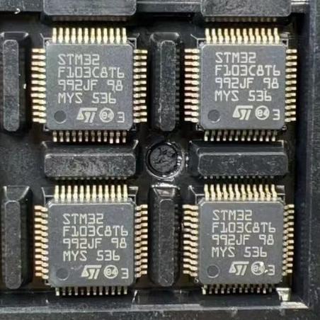
The STM32F103C8T6 operates as a mainstream embedded microcontroller with the following subsystem architecture:
1. Cortex-M3 Core: The 32-bit ARM Cortex-M3 CPU executes at up to 72 MHz, featuring 3-stage pipeline, single-cycle multiplication, hardware division, and 1.25 DMIPS/MHz performance. NVIC (Nested Vectored Interrupt Controller) supports up to 43 maskable interrupt channels with 16 priority levels. The core supports Sleep, Deep-Sleep, and Standby low-power entry via WFI/WFE instructions.
2. Memory Subsystem: 64 KB Flash with prefetch buffer and ART-like acceleration for 0-wait-state execution at 72 MHz (for LQFP48 medium-density devices). 20 KB SRAM is accessible in a single cycle. A 7-channel DMA controller handles peripheral-to-memory and memory-to-memory transfers without CPU intervention.
3. Clock System: Multi-clock source system: HSE (4-16 MHz external crystal), HSI (8 MHz internal RC, 1% accuracy), LSE (32.768 kHz for RTC), LSI (40 kHz for IWDG). A PLL multiplies the clock source to generate the 72 MHz system clock. Clock security system (CSS) detects HSE failure and auto-switches to HSI.
4. Analog Subsystem: Two independent 12-bit successive-approximation ADCs with up to 10 external channels each (ADC1 has additional internal channels for temperature sensor and VREFINT). Maximum sampling rate is 1 MSPS at 14 MHz ADC clock. Dual sample-and-hold capability enables simultaneous sampling.
5. Timer Subsystem: One advanced-control timer (TIM1) for motor control PWM with complementary outputs and dead-time insertion. Three general-purpose 16-bit timers (TIM2-TIM4) for input capture, output compare, PWM generation, and encoder interface. Two basic timers (TIM6-TIM7) for DAC triggering and timebase. SysTick for OS tick generation.
6. Communication Subsystem: All peripherals connected via APB1 (36 MHz max) and APB2 (72 MHz max) buses. USART1 on APB2 (high-speed), USART2/3 on APB1. SPI1 on APB2, SPI2 on APB1. I2C1/2 on APB1. CAN and USB on APB1. Pin multiplexing allows flexible peripheral-to-pin assignment.





 English
  简体中文
简体中文  Español
  العربية