S34ML01G200TFI000


1Gb SLC NAND 闪存、128Mx8、2KB 页、ONFI 1.0、2.7-3.6V、TSOP-48、100K 周期、4 位 ECC、工业 -40~85C

1108

有效库存
转到查询

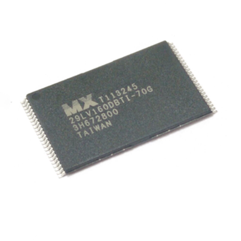
Image for reference only

制造商零件:

S34ML01G200TFI000

包装:

TSOP-I-48(12.00 x 18.40 x 1.00 毫米,0.5 毫米间距)

品牌:
您可能感兴趣的其他建议.
说明

The S34ML01G200TFI000 from SkyHigh Memory (formerly Spansion/Cypress) is a 1Gb (128MB) SLC NAND Flash memory device in a 48-pin TSOP-I package (12.00 x 18.40 mm). It belongs to the S34ML01G2 series (ML-2 family). Organization: 128M x 8 bits. Page size: (2048 + 64) bytes (2KB + 64-byte spare). Block size: 64 pages = (128K + 4K) bytes. Device architecture: 1 plane with 1024 blocks. Supply voltage: VCC = 2.7V to 3.6V (3.3V nominal). Interface: parallel asynchronous NAND with multiplexed address/data/command bus (I/O[7:0]). ONFI 1.0 compliant. Access time: 25ns. Active read current: 30mA. Standby current: 50uA. Program time: 300us typical per page. Erase time: 3.5ms typical per block. Endurance: 100,000 program/erase cycles typical. 4-bit ECC required. Features: Copy Back Program, Read Cache, One-Time Programmable (OTP) area, hardware program/erase protection via WP# pin, unique serial number. Operating temperature: -40C to +85C (industrial). Active product, RoHS compliant. ECCN: 3A991.b.1.a.

The S34ML01G200TFI000 from SkyHigh Memory is a 1-gigabit (128-megabyte) SLC (Single-Level Cell) NAND Flash memory device designed for embedded applications requiring reliable non-volatile data storage. Originally developed by Spansion (later acquired by Cypress Semiconductor and subsequently transferred to SkyHigh Memory), this device represents a mature and well-characterized SLC NAND technology that offers superior endurance and data retention compared to MLC (Multi-Level Cell) alternatives.

SLC NAND stores one bit per cell, providing several key advantages over MLC and TLC NAND: (1) significantly higher program/erase endurance (100,000 cycles typical vs 3,000-10,000 for MLC), (2) better data retention (typically 10+ years at rated temperature), (3) more consistent performance under varying conditions, and (4) simpler error correction requirements (4-bit ECC vs 24+ bits for MLC). These characteristics make SLC NAND the preferred choice for industrial, automotive, and embedded applications where reliability is paramount.

The device is organized as 128M x 8 bits, with the memory array divided into 1024 blocks, each containing 64 pages. Each page consists of a 2048-byte data area and a 64-byte spare area. The spare area is typically used for error correction code (ECC) parity data, wear-leveling metadata, and bad block markers. A minimum of 4-bit ECC per 512-byte sector is required for reliable operation, which can be implemented in software or using a hardware ECC engine in the NAND controller.

The parallel NAND interface uses an 8-bit multiplexed bus (I/O[7:0]) for commands, addresses, and data. The interface is controlled by five signals: CE# (chip enable), CLE (command latch enable), ALE (address latch enable), WE# (write enable), and RE# (read enable). An additional R/B# (ready/busy) output indicates when the device is processing an internal operation (program, erase, or read transfer) and cannot accept new commands. This standard NAND interface is compatible with ONFI 1.0 (Open NAND Flash Interface), ensuring interoperability with compliant NAND controllers.

The device supports Copy Back Program, which allows data to be copied from one page to another within the same device without transferring the data through the external bus. This feature significantly speeds up wear-leveling and garbage collection operations in Flash Translation Layer (FTL) software. The Read Cache feature allows sequential page reads to overlap with data transfer, improving sustained read throughput.

Hardware write protection is provided through the WP# (write protect) pin. When WP# is driven low, all program and erase operations are inhibited, preventing accidental data modification during power transitions or system resets. The internal pull-down on the WP# pin ensures protection even if the pin is left floating.

The One-Time Programmable (OTP) area provides a small region of memory that can be programmed once and permanently locked, useful for storing device-unique calibration data, encryption keys, or serial numbers. A unique serial number is also available in a separate register, enabling device identification for inventory management and anti-counterfeiting.

The TSOP-I-48 package is the industry-standard footprint for NAND Flash, providing a proven and reliable form factor that is compatible with existing PCB layouts and manufacturing processes. The 0.5mm pin pitch supports automated assembly while maintaining a reasonable board area. For space-constrained applications, the device is also available in a 63-ball BGA package (S34ML01G200BHI000).
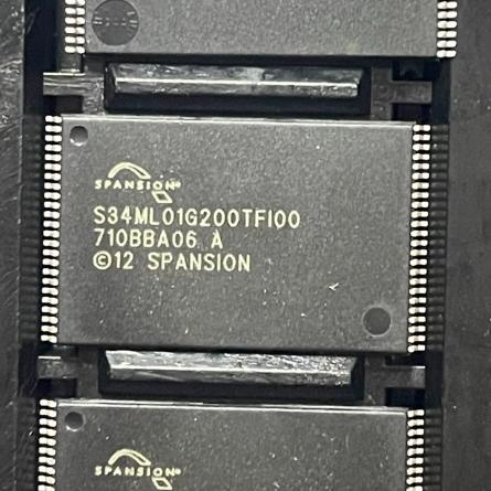

The S34ML01G200TFI000 operates as an asynchronous parallel NAND Flash memory with a multiplexed command/address/data bus.

Memory Array Architecture: The 1Gb memory array is organized as 1024 blocks, each containing 64 pages. Each page consists of a 2048-byte data area and a 64-byte spare area. The total capacity is 1024 blocks x 64 pages x (2048 + 64) bytes = 132,120,576 bytes (approximately 126MB including spare). Blocks are the smallest erasable unit (a block must be fully erased before any page within it can be programmed), while pages are the smallest programmable and readable unit. This two-level hierarchy (block for erase, page for program/read) is fundamental to all NAND Flash architectures.

NAND Interface Protocol: Communication with the device follows a command-based protocol over the 8-bit multiplexed I/O bus. Operations consist of one or more bus cycles: (1) Command cycle: CLE=HIGH, WE# rising edge latches the command byte into the command register. (2) Address cycle: ALE=HIGH, WE# rising edge latches address bytes into the address register. The 1Gb device requires 4 address cycles (column address 1 byte + row address 3 bytes). (3) Data input cycle: CLE=LOW, ALE=LOW, WE# rising edge latches data bytes into the data register/cache. (4) Data output cycle: CLE=LOW, ALE=LOW, RE# falling edge outputs data bytes from the data register.

Page Read Operation: A page read is initiated by writing the Read command (00h-30h) followed by the page address. The device then transfers the entire page from the NAND array to the internal data register, indicated by R/B# going LOW. This transfer time (tR) is typically 25us. Once R/B# goes HIGH, the data can be read out sequentially by toggling RE#. Sequential page reads (Read Cache) allow the next page to be transferred while the current page data is being read out, improving throughput.

Page Program Operation: A page program is initiated by writing the Program Setup command (80h) followed by the page address and up to 2112 bytes of data (2048 data + 64 spare). The Program Execute command (10h) triggers the internal program operation, during which R/B# goes LOW. The typical program time (tPROG) is 300us. After R/B# goes HIGH, the Read Status command (70h) must be issued to check whether the program succeeded (bit 0 = 0) or failed (bit 0 = 1). A failed program typically indicates a bad block that should be retired.

Block Erase Operation: A block erase is initiated by writing the Erase Setup command (60h) followed by the block address (row address only, 3 cycles). The Erase Execute command (D0h) triggers the erase operation, during which R/B# goes LOW. The typical erase time (tBERS) is 3.5ms. After completion, the status register indicates success or failure. Erase can only be performed on a complete block (64 pages); partial block erase is not supported.

Error Correction: SLC NAND requires a minimum of 1-bit ECC per 512 bytes for normal operation, but 4-bit ECC per 512 bytes is recommended to handle the statistical probability of bit errors that accumulate over program/erase cycles and data retention time. The ECC is computed and stored in the spare area during programming, and verified during reading. If the ECC engine detects correctable errors (up to 4 bits per 512-byte sector), it corrects them transparently. If uncorrectable errors are detected, the block should be marked as bad and retired.

Bad Block Management: NAND Flash devices may contain factory-marked bad blocks (indicated by non-FFh data in the spare area of the first page of each bad block). The system software must maintain a bad block table and avoid using these blocks. During operation, blocks that develop uncorrectable errors should also be marked as bad. A wear-leveling algorithm distributes program/erase cycles evenly across all good blocks to maximize the device lifetime.

Write Protection: The WP# pin provides hardware write protection. When WP# is LOW, program and erase commands are ignored. When WP# transitions LOW during a program or erase operation, the operation is aborted (equivalent to a Reset command). The internal pull-down on WP# ensures that program/erase is disabled if the pin is left floating, providing a safe default state.

针脚 名称 类型 说明
1-7, 15-23, 31-39, 47-48 北卡罗来纳州 - No connect; leave floating or tie to GND; these pins are reserved for higher-density devices in the same package (S34ML02G2, S34ML04G2) or for x16 bus width configuration
8 I/O0 输入/输出 Data/Address/Command bit 0 (LSB); multiplexed bus; input during command, address, and data input cycles; output during data read cycles; high-impedance when CE#=HIGH or RE#=HIGH
9 I/O1 输入/输出 Data/Address/Command bit 1
10 I/O2 输入/输出 Data/Address/Command bit 2
11 I/O3 输入/输出 Data/Address/Command bit 3
12 VSS 地面 接地;连接至 PCB 地平面
13 I/O4 输入/输出 Data/Address/Command bit 4
14 I/O5 输入/输出 Data/Address/Command bit 5
24 I/O6 输入/输出 Data/Address/Command bit 6
25 I/O7 输入/输出 Data/Address/Command bit 7 (MSB); also serves as status bit 7 (write protect status) during Read Status command
26 VCC 电源 Device power supply; 2.7V to 3.6V; decouple with 0.1uF ceramic capacitor to VSS close to the device; connect to clean 3.3V power rail
27 VSS 地面 接地;连接至 PCB 地平面
28 CE# 输入 Chip Enable; active LOW; LOW selects the device for bus operations; HIGH deselects the device (I/O pins go high-impedance, internal logic enters standby); must be LOW during all command, address, and data transfers
29 CLE 输入 Command Latch Enable; HIGH during command input cycles; the command on I/O[7:0] is latched into the command register on the rising edge of WE# when CLE is HIGH
30 ALE 输入 Address Latch Enable; HIGH during address input cycles; the address on I/O[7:0] is latched into the address register on the rising edge of WE# when ALE is HIGH
40 WE# 输入 Write Enable; commands, addresses, and input data are latched on the rising edge of WE#; must be HIGH during read operations
41 WP# 输入 Write Protect; active LOW; LOW inhibits all program and erase operations; LOW during active program/erase aborts the operation (equivalent to Reset); internal pull-down ensures protection if pin floats; tie to VCC through a resistor to enable program/erase
42 R/B# Open-Drain Output Ready/Busy output; active LOW (busy); LOW indicates the device is processing an internal operation (program, erase, read transfer); HIGH indicates the device is ready for the next command; open-drain requires external pull-up resistor (10kOhm typical); can be wire-ORed with other NAND devices
43 RE# 输入 Read Enable; data is output on the falling edge of RE#; each RE# falling edge increments the internal column address counter; must be HIGH during write operations
应用 说明
Embedded Linux Boot Storage Store bootloader, kernel, and root filesystem for embedded Linux systems; 128MB capacity sufficient for compact Linux distributions; SLC endurance (100K cycles) ensures long service life under frequent writes; 4-bit ECC meets Linux kernel MTD subsystem requirements; ONFI 1.0 compatibility ensures standard NAND controller support
Industrial Data Logging Record sensor data and event logs in industrial environments; SLC endurance handles frequent write cycles; 25ns access time supports fast data capture; wide temperature range (-40C to +85C) for harsh environments; WP# hardware protection prevents accidental data erasure
Consumer Electronics Firmware Store firmware and configuration data for routers, set-top boxes, and smart home devices; 128MB provides ample space for firmware images and backup copies; Copy Back Program enables fast firmware updates; OTP area stores device-unique calibration data
汽车信息娱乐系统 Store navigation maps, media files, and system firmware in automotive head units; SLC reliability ensures data integrity under temperature cycling; Read Cache improves sequential read throughput for map rendering; industrial temperature range (extended grade -40C to +125C available in other SKUs)
Medical Device Storage Store patient data and device calibration in medical equipment; SLC provides highest data reliability among NAND types; 100K cycle endurance handles frequent data updates; WP# pin ensures compliance with data protection requirements
模型 制造商 兼容性 主要区别
S34ML01G200BHI000 天高内存 Same in BGA Package Identical 1Gb SLC NAND in 63-ball BGA package (9x11mm); smaller footprint; better signal integrity at high speeds; use when TSOP footprint is too large or for new designs requiring BGA
S34ML02G200TFI000 天高内存 Higher Density, Same Package 2Gb (256MB) SLC NAND in same TSOP-48 pinout; same page size (2KB+128 spare); 2 planes; supports multi-plane program/erase; drop-in upgrade with firmware change; same VCC and interface
S34ML04G200TFI000 天高内存 Higher Density, Same Package 4Gb (512MB) SLC NAND in same TSOP-48 pinout; 2 planes with 2048 blocks; multi-plane operations; drop-in upgrade with firmware change; highest density in the family
MT29F1G01ABAFDSF-IT:F 美光 功能等同 1Gb SLC NAND in TSOP-48; different command set (not ONFI); different spare area size; requires firmware adaptation for command differences; Micron-specific ECC requirements
TC58NVG0S3HTA00 基奥夏(东芝) 功能等同 1Gb SLC NAND in TSOP-48; similar page/block architecture; different command set; requires firmware adaptation; different manufacturer ID
推荐部件
质量保证

我们从合作供应链采购的所有电子元件都经过严格的进货检验。通过仔细的测试,我们确保交付给客户的所有产品都是原装正品,符合质量要求。此外,我们还保存完整的检验记录,使整个供应链流程清晰可查。.

认证
我们获得了多项专业认证,并建立了自己的专业检测实验室,确保交付给客户的每一件产品都符合最高质量要求。我们严格按照流程进行检测,确保产品质量稳定、参数准确。为保证原装正品,我们还与可靠的第三方检测机构合作,进行严格的质量检测。我们始终高度重视质量,完全符合行业标准、相关法规和 ISO 9001:2015 的要求。.

发货与付款

我们从合作供应链采购的所有电子元件都经过严格的进货检验。通过仔细的测试,我们确保交付给客户的所有产品都是原装正品,符合质量要求。此外,我们还保存完整的检验记录,使整个供应链流程清晰可查。.

认证
我们获得了多项专业认证,并建立了自己的专业检测实验室,确保交付给客户的每一件产品都符合最高质量要求。我们严格按照流程进行检测,确保产品质量稳定、参数准确。为保证原装正品,我们还与可靠的第三方检测机构合作,进行严格的质量检测。我们始终高度重视质量,完全符合行业标准、相关法规和 ISO 9001:2015 的要求。.

服务与包装

我们从合作供应链采购的所有电子元件都经过严格的进货检验。通过仔细的测试,我们确保交付给客户的所有产品都是原装正品,符合质量要求。此外,我们还保存完整的检验记录,使整个供应链流程清晰可查。.

认证
我们获得了多项专业认证,并建立了自己的专业检测实验室,确保交付给客户的每一件产品都符合最高质量要求。我们严格按照流程进行检测,确保产品质量稳定、参数准确。为保证原装正品,我们还与可靠的第三方检测机构合作,进行严格的质量检测。我们始终高度重视质量,完全符合行业标准、相关法规和 ISO 9001:2015 的要求。.