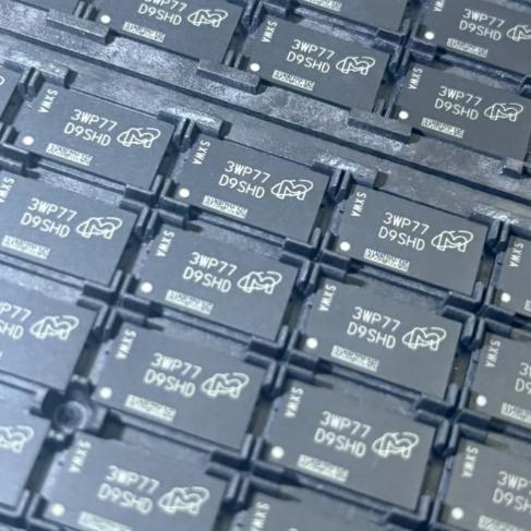
MT41K256M16TW-107:P


4Gbit DDR3L SDRAM,1866 MT/秒,1.35V,96 球 FBGA

3856

有效库存
转到查询

Image for reference only

制造商零件:

MT41K256M16TW-107:P

包装:

96 球 FBGA(8 毫米 x 14 毫米 x 0.92 毫米)

品牌:
您可能感兴趣的其他建议.
说明

The MT41K256M16TW-107:P is a 4Gbit (256M x 16) DDR3L SDRAM manufactured by Micron Technology, operating at 1.35V with backward compatibility to 1.5V DDR3 platforms. It features an 8n-prefetch double data rate architecture supporting 1866 MT/s data rate (933 MHz clock) with CL=13 timing. The device incorporates 8 internal banks for concurrent operation, nominal and dynamic on-die termination (ODT), differential data strobe (DQS/DQS#), programmable CAS latency, burst length of 8 with burst chop 4 on-the-fly selection, self-refresh with temperature-compensated auto-refresh, write leveling, and ZQ calibration. Fabricated in 20nm process and packaged in a 96-ball FBGA (8mm x 14mm), it operates over the commercial temperature range of 0°C to 95°C, making it suitable for embedded computing, networking equipment, industrial automation, consumer electronics, and automotive infotainment systems.

The MT41K256M16TW-107:P is a 4Gbit (512MB) DDR3L SDRAM device manufactured by Micron Technology, organized as 256 Meg x 16 bits. It belongs to the MT41K series of low-voltage DDR3 SDRAM devices, operating at VDD = VDDQ = 1.35V (range: 1.283V to 1.45V) while maintaining backward compatibility with 1.5V DDR3 applications. The device uses an 8n-prefetch architecture with a double data rate interface that transfers two data words per clock cycle at the I/O pins.

The -107 speed grade supports a maximum clock frequency of 933 MHz (1866 MT/s data rate) with CL = 13 timing (tRCD = 13.91ns, tRP = 13.91ns). The device incorporates 8 internal banks for concurrent operation, enabling high bandwidth by hiding row precharge and activation time. It features nominal and dynamic on-die termination (ODT) for data, strobe, and mask signals, differential bidirectional data strobe (DQS/DQS#), and differential clock inputs (CK/CK#).

Fabricated in 20nm process technology, the device is packaged in a 96-ball FBGA (8mm x 14mm, height 0.92mm) with commercial temperature range (0°C to 95°C). Key features include programmable CAS latency (CL), programmable posted CAS additive latency (AL), programmable CAS write latency (CWL), fixed burst length of 8 (BL8) and burst chop of 4 (BC4) with on-the-fly selection, self-refresh mode with temperature-compensated auto-refresh, write leveling, multipurpose register, and output driver calibration via ZQ pin. The device supports refresh intervals of 64ms at 0-85°C and 32ms at 85-95°C with 8192 refresh cycles.

The MT41K256M16TW-107:P employs a double data rate (DDR) architecture based on an 8n-prefetch scheme. A single read or write operation consists of a single 8n-bit-wide, four-clock-cycle data transfer at the internal DRAM core, paired with eight corresponding n-bit-wide, one-half-clock-cycle data transfers at the I/O pins. This architecture enables high bandwidth while keeping the internal DRAM core frequency at one-eighth of the external data rate.

Clock and Command Subsystem: The device operates from differential clock inputs (CK and CK#). All control, command, and address signals are registered at the positive edge of CK. Commands are decoded from the CS#, RAS#, CAS#, WE#, and ACT# pins to initiate operations such as ACTIVATE, READ, WRITE, PRECHARGE, REFRESH, and mode register access.

Memory Array Subsystem: The 4Gbit density is organized as 256 Meg x 16 with 8 internal banks. Each bank contains 32K rows (A[14:0]), 1K columns (A[9:0]), and a 2KB page size. The 8-bank architecture allows concurrent bank operations, hiding row access latency through bank interleaving and improving overall throughput.

Data Path Subsystem: Data is transferred via the 16-bit DQ bus with differential data strobe signals (DQS/DQS#). During WRITE operations, DQS is center-aligned with data for reliable capture. During READ operations, the DRAM transmits data edge-aligned to DQS. The device supports BL8 (burst length 8) and BC4 (burst chop 4) with on-the-fly selection via the mode register.

On-Die Termination (ODT) Subsystem: The device supports both nominal and dynamic ODT for DQ, DQS, DQS#, and DM signals. ODT values are programmable through mode registers (RTT_NOM, RTT_WR), providing signal integrity optimization without external termination components. Dynamic ODT allows the termination value to change on-the-fly during write operations.

Refresh Subsystem: The device requires 8192 refresh commands every 64ms (0-85°C) or 32ms (85-95°C). Self-refresh mode with auto-refresh (SRT) enables autonomous refresh operation during low-power standby. The ZQ calibration subsystem performs periodic output driver impedance calibration against an external 240-ohm resistor to maintain signal integrity over temperature and voltage variations.

别针组 Pin / Ball 类型 默认功能 说明
时钟 CK, CK# I Differential Clock Input All commands are latched on the rising edge of CK
Chip Select CS# I Chip Select (Active Low) Enables or disables the command decoder
Command RAS#, CAS#, WE# I Command Inputs Define the command being entered along with CS#
Activate ACT# I Activate Input Activates the specified row in the selected bank
Address A[14:0] I Address Inputs Provide row and column address; also used for mode register set and burst chop
Bank Address BA[2:0] I Bank Select Select which bank is active for READ, WRITE, or ACTIVATE
Data DQ[15:0] 输入/输出 Data Bus Bi-directional data bus, 16-bit wide
数据选通 DQS, DQS# 输入/输出 Differential Data Strobe Bi-directional differential strobe for data capture
Data Mask DM I Data Mask Input Masks write data; sampled during write operations
ODT ODT I On-Die Termination Enable Enables ODT for DQ/DQS/DM signals during reads
Clock Enable CKE I Clock Enable (Active High) Enables internal clock signals and device operation
重置 RESET# I Active Low Reset Asynchronous reset; clears all internal state
Calibration ZQ I Impedance Calibration Reference Connected to external 240-ohm resistor for ODT/driver calibration
电源 VDD P Core Power Supply 1.35V nominal (1.283V – 1.45V)
电源 VDDQ P I/O Power Supply 1.35V nominal (1.283V – 1.45V)
电源 VREFCA P Reference Voltage (CA) Command/Address reference voltage = VDD/2
电源 VREFDQ P Reference Voltage (DQ) Data reference voltage = VDDQ/2
地面 VSS G 地面 Device ground connections
Application Scenario Role of MT41K256M16TW-107:P Key Features Utilized Typical Pairing
Embedded Computing (ARM/FPGA Systems) Main system memory providing 512MB capacity with high bandwidth for processor code execution and data buffering 1866 MT/s data rate, 16-bit bus width, low 1.35V power, ODT for signal integrity ARM Cortex-A series SoC (e.g., i.MX8, RK3399), FPGA (e.g., Xilinx Zynq UltraScale+)
Networking and Telecom Equipment Packet buffering and lookup table storage in routers, switches, and baseband processors 8-bank interleaving for concurrent access, BC4/BL8 on-the-fly, high MT/s throughput Network SoC (e.g., NXP Layerscape), Ethernet switch ASIC
Industrial Automation and HMI Operating system memory for industrial PCs, PLCs, and HMI panels requiring reliable DRAM in commercial temperature range Self-refresh with auto-refresh (SRT), ZQ calibration, 0-95°C operation Industrial MCU/MPU (e.g., TI Sitara, STM32MP1)
Consumer Electronics (Smart TV, STB) Video frame buffer and application memory in smart TVs, set-top boxes, and streaming devices 256Mx16 organization, low standby current, backward compatible with 1.5V DDR3 platforms Media SoC (e.g., Realtek RTD1319, Amlogic S905X4)
Automotive Infotainment (Non-Safety) System memory for in-vehicle infotainment (IVI) and navigation systems at commercial temperature grade 1.35V low-power operation, write leveling, programmable ODT Automotive SoC (e.g., Renesas R-Car, NXP i.MX8XL)
模型 Compatibility Type Compatibility Level Key Differences 制造商
AS4C256M16D3-12BCN 功能相似 Partially Compatible DDR3L 256Mx16, 1600 MT/s (slower), 96-ball FBGA, timing differences require firmware adjustment Alliance Memory
IS46TR16256AL-15HBLA1-TR 功能相似 Partially Compatible DDR3L 256Mx16, 1333 MT/s, 96-ball FBGA, lower speed grade, requires timing reconfiguration ISSI
MT41K256M16TW-107 IT:P 系列变体 Fully Compatible Industrial temp range (-40°C to 95°C), same speed grade and pinout, direct drop-in replacement for wider temp range 美光
MT41K256M16TW-107 AIT:P 系列变体 Fully Compatible Automotive grade (AEC-Q100), -40°C to 95°C, higher unit price ($7.66+), same pinout and functionality 美光
W632GU6MB-12 功能相似 Partially Compatible DDR3L 256Mx16, 1600 MT/s, 96-ball FBGA, lower speed, different timing parameters Winbond
EM6AB16CWKG-12H 功能相似 Partially Compatible DDR3L 256Mx16, 1600 MT/s, 96-ball FBGA, lower data rate, requires timing and mode register adjustments Etron Technology
推荐部件
4GB eMMC 5.1, HS400, 153-VFBGA, integrated controller, industrial temp

品牌:

封装:

153-VFBGA (11.5 x 13.0 x 1.0 mm)
有库存:
11847pcs

货运周期:3~7 天
最低订购量为 1

转到查询
4Gb (512MB) SLC NAND 闪存,x8,3.3V,TSOP-48,2K+64 页,128K 块,100K 周期,异步,ONFI 1.0,内部 4 位 ECC,0~70C

品牌:

封装:

48 引脚 TSOP I 型(12 x 18.4 x 1.0 毫米,0.5 毫米间距)
有库存:
1162 件

货运周期:3~7 天
最低订购量为 1

转到查询
2Gb SLC NAND 闪存,x8,ONFI 1.0,3.3V,TSOP-48,内部 4 位 ECC,商用温度

品牌:

封装:

TSOP-I-48(18.4 x 12 毫米)
有库存:
2004 件

货运周期:3~7 天
最低订购量为 1

转到查询
质量保证

我们从合作供应链采购的所有电子元件都经过严格的进货检验。通过仔细的测试,我们确保交付给客户的所有产品都是原装正品,符合质量要求。此外,我们还保存完整的检验记录,使整个供应链流程清晰可查。.

认证
我们获得了多项专业认证,并建立了自己的专业检测实验室,确保交付给客户的每一件产品都符合最高质量要求。我们严格按照流程进行检测,确保产品质量稳定、参数准确。为保证原装正品,我们还与可靠的第三方检测机构合作,进行严格的质量检测。我们始终高度重视质量,完全符合行业标准、相关法规和 ISO 9001:2015 的要求。.

发货与付款

我们从合作供应链采购的所有电子元件都经过严格的进货检验。通过仔细的测试,我们确保交付给客户的所有产品都是原装正品,符合质量要求。此外,我们还保存完整的检验记录,使整个供应链流程清晰可查。.

认证
我们获得了多项专业认证,并建立了自己的专业检测实验室,确保交付给客户的每一件产品都符合最高质量要求。我们严格按照流程进行检测,确保产品质量稳定、参数准确。为保证原装正品,我们还与可靠的第三方检测机构合作,进行严格的质量检测。我们始终高度重视质量,完全符合行业标准、相关法规和 ISO 9001:2015 的要求。.

服务与包装

我们从合作供应链采购的所有电子元件都经过严格的进货检验。通过仔细的测试,我们确保交付给客户的所有产品都是原装正品,符合质量要求。此外,我们还保存完整的检验记录,使整个供应链流程清晰可查。.

认证
我们获得了多项专业认证,并建立了自己的专业检测实验室,确保交付给客户的每一件产品都符合最高质量要求。我们严格按照流程进行检测,确保产品质量稳定、参数准确。为保证原装正品,我们还与可靠的第三方检测机构合作,进行严格的质量检测。我们始终高度重视质量,完全符合行业标准、相关法规和 ISO 9001:2015 的要求。.



