AT45DB321E-SHF-T


32Mbit DataFlash,带双 SRAM 缓冲器,256 字节页面擦除,SPI 85MHz,SOIC-8,-40~85C,寿命长达 2034 年

5862

有效库存
转到查询

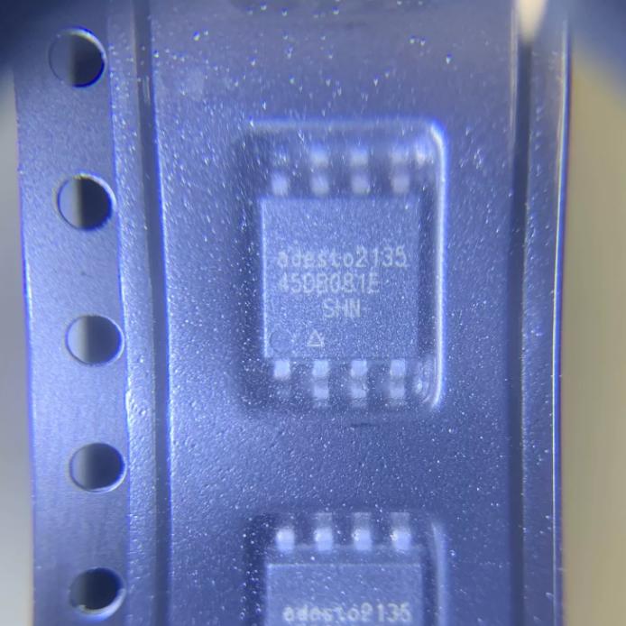
Image for reference only

制造商零件:

AT45DB321E-SHF-T

包装:

SOIC-8 208 密耳(5.18 x 7.70 x 1.8 毫米)

品牌:
您可能感兴趣的其他建议.
说明

The AT45DB321E-SHF-T from Renesas Electronics (formerly Adesto) is a 32Mbit (4MB) DataFlash serial Flash memory in SOIC-8 (208-mil) package, operating from 2.3V to 3.6V. It features a unique dual SRAM buffer architecture with two 256/264-byte buffers enabling simultaneous read-while-write and page-erase-as-small-as-256-bytes for efficient data logging. The device supports SPI Mode 0 and Mode 3 at clock frequencies up to 85MHz. Memory organization: 8,192 pages of 528 bytes (standard) or 8,192 pages of 512 bytes (binary). Page program time: 4ms. Active read current: 6mA (typical). Ultra-deep power-down: 0.4uA. Byte-write capability provides serial EEPROM functionality. Comprehensive security features include sector lockdown, write protect, and unique 64-bit ID. -40C to 85C. MSL-1, RoHS3. Tape and reel, 2250/reel. Product longevity guaranteed to 2034.

The AT45DB321E-SHF-T is a 32Mbit (4M x 8) DataFlash serial Flash memory from Renesas Electronics (formerly Adesto Technology), housed in an 8-pin SOIC 208-mil package. The device belongs to the System Enhancing class of code and data storage solutions, distinguished by its advanced dual SRAM buffer architecture that makes it the most efficient memory for data logging applications.

The AT45DB321E features two independent SRAM data buffers (each 256 or 264 bytes depending on page size mode) that enable simultaneous read-while-write operations: while data is being programmed from one buffer to the main memory, new data can be loaded into the other buffer. This dual-buffer architecture eliminates the programming wait time that single-buffer Flash memories require, dramatically improving data throughput in continuous logging applications.

The memory supports two page size configurations: standard DataFlash page size of 528 bytes (528 x 8,192 pages = 32,030,208 bits + 1,048,576 extra bits) and binary page size of 512 bytes (512 x 8,192 pages = 33,554,432 bits). The page erase granularity of 256 bytes (half-page) is the smallest erase unit available in any serial Flash, providing maximum flexibility for data logging applications where small data records must be updated frequently without erasing large sectors.

The SPI interface supports Mode 0 (CPOL=0, CPHA=0) and Mode 3 (CPOL=1, CPHA=1) at clock frequencies up to 85MHz. The device uses a 4-wire SPI interface: CS (chip select), SCK (serial clock), SI (serial input), and SO (serial output). The WP (write protect) pin provides hardware sector protection, and the RESET pin allows external reset of the internal state machine.

Additional features include: byte-write capability (enabling serial EEPROM-like random byte access), ultra-deep power-down mode (0.4uA typical), comprehensive security features (sector lockdown, write protection, unique 64-bit device ID, security register), and RapidS protocol for high-speed continuous read operations. The device is guaranteed for 100,000 page erase/program cycles per page with 20-year data retention. Renesas guarantees product longevity to 2034.

The SHF suffix denotes: S = SOIC-8 package, H = industrial temperature grade with NiPdAu lead finish, F = 2.3V minimum operating voltage. The T suffix denotes tape and reel packaging (2,250 units per reel). The device is RoHS3 compliant, MSL Level 1, and classified as ECCN 3A991B1A.

The AT45DB321E-SHF-T operates as a page-erase DataFlash serial memory with a dual SRAM buffer architecture, controlled through SPI command sequences from a host microcontroller.

Dual SRAM Buffer Architecture: The key differentiator of the AT45DB321E is its two independent SRAM data buffers (Buffer 1 and Buffer 2), each matching the page size (528 or 512 bytes). These buffers serve as intermediate holding areas between the SPI interface and the main Flash memory array. Data is first written from the SPI bus into a buffer, then programmed from the buffer to the main memory page. This architecture enables three critical capabilities: (1) Read-while-write: while data from Buffer 1 is being programmed into a main memory page, the host can simultaneously read data from Buffer 2 or from a different main memory page; (2) Continuous data logging: new sensor data fills Buffer 2 while Buffer 1 is being programmed, eliminating dead time between measurements; (3) Compare-then-program: data in a buffer can be compared with a main memory page before programming to verify data integrity.

Page Erase and Program: Unlike standard SPI Flash memories that erase in 4KB sectors minimum, the AT45DB321E supports page-level erase (256 or 264 bytes minimum) and even byte-level write within a page. The smallest erase granularity makes it ideal for data logging where small records are updated frequently. The page program time is typically 4ms, and the page erase time is typically 35ms.

SPI Command Protocol: The host communicates by asserting CS LOW, clocking in an 8-bit opcode on SI, followed by address bytes and data as required by the command. Over 40 opcodes support operations including: continuous array read (1Bh for high-frequency mode up to 85MHz), buffer read/write (84h/82h for Buffer 1, 85h/83h for Buffer 2), buffer-to-main-memory program with erase (83h/86h), buffer-to-main-memory program without erase (88h/89h), main-memory-page-to-buffer transfer (53h/55h), main-memory-page-to-buffer compare (60h/61h), auto page rewrite (58h/59h), status register read (D7h), and manufacturer/device ID read (9Fh).

Status Register: The 8-bit status register (read via opcode D7h) provides critical operational status: Bit 7 (RDY/BUSY) indicates whether the device is ready for a new command (1=ready, 0=busy), Bit 6 (COMP) indicates the result of a buffer-to-main-memory compare operation (1=mismatch, 0=match), and Bits 0-1 indicate the page size configuration and sector protection status.

Write Protection: The WP pin provides hardware write protection for sectors configured as protected via the Sector Protection Register. When WP is asserted LOW, any program or erase command to a protected sector is ignored. Sector protection is configured through a separate command sequence and can be permanently locked via the Sector Lockdown command, preventing any future modification. This provides defense-in-depth against accidental or malicious data corruption.

Ultra-Deep Power-Down: The ultra-deep power-down command (79h) reduces current consumption to 0.4uA (typical), significantly lower than the standard deep power-down mode. Exit from ultra-deep power-down requires a dedicated wake command followed by a recovery time. This mode is useful for battery-powered data loggers that spend most of their time in sleep mode between measurement intervals.

针脚 名称 类型 说明
1 /CS 输入 Chip Select; active LOW; asserts device for SPI communication; deasserting CS terminates operation and tri-states SO; must be HIGH during power-up
2 /RESET 输入 Hardware Reset; active LOW; terminates in-progress operation and resets internal state machine to idle; can be left floating with internal pull-up if unused
3 /WP 输入 Write Protect; active LOW; when asserted, prevents program/erase operations on sectors configured as protected via Sector Protection Register; hardware-level protection override
4 接地 电源 接地;连接至系统地平面
5 SI 输入 Serial Data Input; receives opcodes, addresses, and data from host; data latched on rising edge of SCK; ignored when CS is deasserted
6 SCK 输入 Serial Clock; SPI clock input; up to 85MHz; data input on SI sampled on rising edge; data output on SO driven on falling edge; supports Mode 0 and Mode 3
7 SO 输出 Serial Data Output; outputs data during read operations on falling edge of SCK; high-impedance when CS is deasserted or during command input phase
8 VCC 电源 Supply voltage; 2.3V to 3.6V operating range; bypass with 0.1uF ceramic capacitor to GND close to pin
应用 说明
Data Logging Dual SRAM buffers enable continuous logging without programming dead time; 256-byte page erase minimizes Flash wear when updating small records; byte-write for incremental data append; ideal for sensor data acquisition
Industrial Data Recording Page-erase granularity (256 bytes) allows frequent updates of small data records without erasing large 4KB sectors; guaranteed 100K cycles per page; 20-year retention for long-term archival
Embedded Code and Data Storage Continuous array read at 85MHz for fast code execution; dual buffers allow code execution from one buffer while updating data in the other; RapidS protocol for high-speed XIP
Voice/Audio Storage 528-byte page size naturally fits audio compression frame sizes; sequential write through buffers provides continuous recording without gaps; page erase allows segment-level audio management
电池供电设备 Ultra-deep power-down at 0.4uA extends battery life; 2.3V minimum operation supports direct battery connection; 6mA active read current is low for portable applications
模型 制造商 兼容性 主要区别
AT45DB321E-SHF-B 瑞萨 Same Die / Different Packaging Tube packaging (B suffix) instead of tape and reel (T suffix); same SOIC-8 package; same electrical specifications; 2,250 pcs/tube
AT45DB321E-MHF-T 瑞萨 功能相同 UDFN 5x6mm package (M suffix); same 32Mbit DataFlash with dual buffers; smaller footprint for space-constrained designs; different thermal characteristics
AT45DB641E-SHF-T 瑞萨 引脚兼容/同系列 64Mbit (8MB) capacity; same SOIC-8 pinout and dual-buffer architecture; double storage density; same command set
W25Q32JVSSIQ Winbond 功能相似 32Mbit SPI NOR Flash; standard sector-erase (4KB minimum, no 256-byte page erase); no dual SRAM buffers; higher clock (133MHz); different architecture for simpler code storage
MX25L3233FM2I-08G 旺宏 功能相似 32Mbit SPI NOR Flash; SOIC-8; 86MHz; standard 4KB sector erase; no dual-buffer architecture; lower cost for code-only storage without data logging needs
推荐部件
4.5MHz BiMOS Op-Amp, MOSFET input, 4-36V supply, 10pA Ib, PDIP-8

品牌:

封装:

PDIP-8 (9.7 x 6.6 x 3.94 mm)
有库存:
11635pcs

货运周期:3~7 天
最低订购量为 1

转到查询
8Mbit DataFlash、双 SPI 85MHz、2x264B SRAM 缓冲器、USON-8 (4x3mm)、基于页面的 ECC

品牌:

封装:

USON-8(4 x 3 x 0.6 毫米,0.8 毫米间距)
有库存:
4500 件

货运周期:3~7 天
最低订购量为 1

转到查询
64Mbit DataFlash、1.7-3.6V SPI、85MHz、双 SRAM 缓冲器、SOIC-W T/R、工业温度

品牌:

封装:

8 引线 SOIC-W(5.18 x 7.70 毫米,1.27 毫米间距,鸥翼形,0.208 英寸宽)
有库存:
0 件

货运周期:3~7 天
最低订购量为 1

转到查询
1Hz 中断发生器,3.0-3.6V,30µA Iq,TDFN-8 (2x2mm),-40~85°C,无外部元件

品牌:

封装:

带裸露焊盘的 TDFN-8(2.0 x 2.0 x 0.55 毫米,0.5 毫米间距)
有库存:
22000 件

货运周期:3~7 天
最低订购量为 1

转到查询
质量保证

我们从合作供应链采购的所有电子元件都经过严格的进货检验。通过仔细的测试,我们确保交付给客户的所有产品都是原装正品,符合质量要求。此外,我们还保存完整的检验记录,使整个供应链流程清晰可查。.

认证
我们获得了多项专业认证,并建立了自己的专业检测实验室,确保交付给客户的每一件产品都符合最高质量要求。我们严格按照流程进行检测,确保产品质量稳定、参数准确。为保证原装正品,我们还与可靠的第三方检测机构合作,进行严格的质量检测。我们始终高度重视质量,完全符合行业标准、相关法规和 ISO 9001:2015 的要求。.

发货与付款

我们从合作供应链采购的所有电子元件都经过严格的进货检验。通过仔细的测试,我们确保交付给客户的所有产品都是原装正品,符合质量要求。此外,我们还保存完整的检验记录,使整个供应链流程清晰可查。.

认证
我们获得了多项专业认证,并建立了自己的专业检测实验室,确保交付给客户的每一件产品都符合最高质量要求。我们严格按照流程进行检测,确保产品质量稳定、参数准确。为保证原装正品,我们还与可靠的第三方检测机构合作,进行严格的质量检测。我们始终高度重视质量,完全符合行业标准、相关法规和 ISO 9001:2015 的要求。.

服务与包装

我们从合作供应链采购的所有电子元件都经过严格的进货检验。通过仔细的测试,我们确保交付给客户的所有产品都是原装正品,符合质量要求。此外,我们还保存完整的检验记录,使整个供应链流程清晰可查。.

认证
我们获得了多项专业认证,并建立了自己的专业检测实验室,确保交付给客户的每一件产品都符合最高质量要求。我们严格按照流程进行检测,确保产品质量稳定、参数准确。为保证原装正品,我们还与可靠的第三方检测机构合作,进行严格的质量检测。我们始终高度重视质量,完全符合行业标准、相关法规和 ISO 9001:2015 的要求。.



