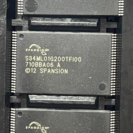
The S34ML01G200TFI000 from SkyHigh Memory is a 1-gigabit (128-megabyte) SLC (Single-Level Cell) NAND Flash memory device designed for embedded applications requiring reliable non-volatile data storage. Originally developed by Spansion (later acquired by Cypress Semiconductor and subsequently transferred to SkyHigh Memory), this device represents a mature and well-characterized SLC NAND technology that offers superior endurance and data retention compared to MLC (Multi-Level Cell) alternatives.
SLC NAND stores one bit per cell, providing several key advantages over MLC and TLC NAND: (1) significantly higher program/erase endurance (100,000 cycles typical vs 3,000-10,000 for MLC), (2) better data retention (typically 10+ years at rated temperature), (3) more consistent performance under varying conditions, and (4) simpler error correction requirements (4-bit ECC vs 24+ bits for MLC). These characteristics make SLC NAND the preferred choice for industrial, automotive, and embedded applications where reliability is paramount.
The device is organized as 128M x 8 bits, with the memory array divided into 1024 blocks, each containing 64 pages. Each page consists of a 2048-byte data area and a 64-byte spare area. The spare area is typically used for error correction code (ECC) parity data, wear-leveling metadata, and bad block markers. A minimum of 4-bit ECC per 512-byte sector is required for reliable operation, which can be implemented in software or using a hardware ECC engine in the NAND controller.
The parallel NAND interface uses an 8-bit multiplexed bus (I/O[7:0]) for commands, addresses, and data. The interface is controlled by five signals: CE# (chip enable), CLE (command latch enable), ALE (address latch enable), WE# (write enable), and RE# (read enable). An additional R/B# (ready/busy) output indicates when the device is processing an internal operation (program, erase, or read transfer) and cannot accept new commands. This standard NAND interface is compatible with ONFI 1.0 (Open NAND Flash Interface), ensuring interoperability with compliant NAND controllers.
The device supports Copy Back Program, which allows data to be copied from one page to another within the same device without transferring the data through the external bus. This feature significantly speeds up wear-leveling and garbage collection operations in Flash Translation Layer (FTL) software. The Read Cache feature allows sequential page reads to overlap with data transfer, improving sustained read throughput.
Hardware write protection is provided through the WP# (write protect) pin. When WP# is driven low, all program and erase operations are inhibited, preventing accidental data modification during power transitions or system resets. The internal pull-down on the WP# pin ensures protection even if the pin is left floating.
The One-Time Programmable (OTP) area provides a small region of memory that can be programmed once and permanently locked, useful for storing device-unique calibration data, encryption keys, or serial numbers. A unique serial number is also available in a separate register, enabling device identification for inventory management and anti-counterfeiting.
The TSOP-I-48 package is the industry-standard footprint for NAND Flash, providing a proven and reliable form factor that is compatible with existing PCB layouts and manufacturing processes. The 0.5mm pin pitch supports automated assembly while maintaining a reasonable board area. For space-constrained applications, the device is also available in a 63-ball BGA package (S34ML01G200BHI000).





 English
  简体中文
简体中文  Español
  العربية