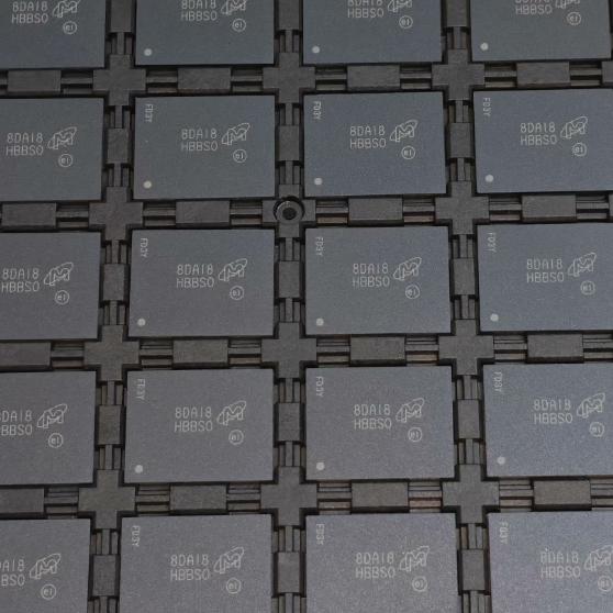
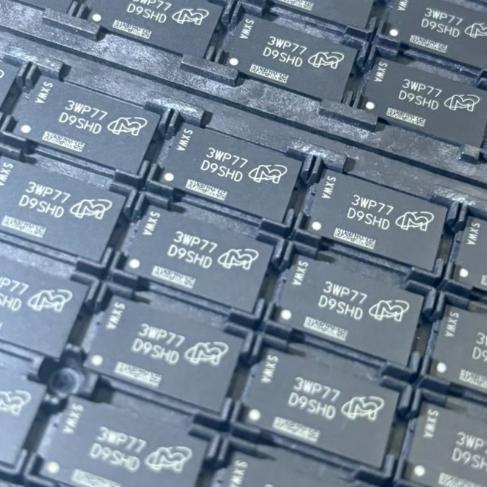
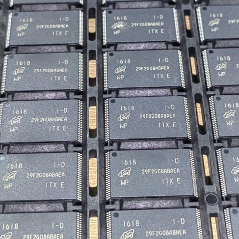
MT29F2G08ABAAWP:E


2Gb SLC NAND 闪存,x8,ONFI 1.0,3.3V,TSOP-48,内部 4 位 ECC,商用温度

2004

有效库存
转到查询

Image for reference only

制造商零件:

MT29F2G08ABAAWP:E

包装:

TSOP-I-48(18.4 x 12 毫米)

品牌:
您可能感兴趣的其他建议.
说明

The MT29F2G08ABAEAWP:E is a 2Gb (256MB) SLC NAND Flash from Micron Technology in a 48-pin TSOP-I package. It features an x8 parallel asynchronous interface compliant with ONFI 1.0, with internal 4-bit ECC, 2,048 blocks of 64 pages (2,112 bytes each), page read time of 25 µs, program time of 200 µs, and erase time of 700 µs. The device supports two-plane operations, program/read cache mode, internal data move, and OTP. Operating at 2.7V-3.6V with 35 mA max current, it delivers 100,000 P/E cycle endurance and 10-year data retention. Commercial temperature range: 0°C to +70°C. MSL-3 rated, RoHS compliant, ECCN 3A991.b.1.a.

The MT29F2G08ABAEAWP:E is a 2-gigabit (256MB) single-level cell (SLC) NAND Flash memory device manufactured by Micron Technology. It uses an 8-bit wide (x8) parallel asynchronous interface and is compliant with the Open NAND Flash Interface (ONFI) 1.0 specification. The device is organized as 256M x 8 bits, with 2,048 blocks, each containing 64 pages of 2,112 bytes (2,048 data + 64 spare bytes).

As an SLC NAND device, the MT29F2G08ABAEAWP:E delivers superior endurance and reliability compared to MLC or TLC alternatives, with 100,000 program/erase cycles and 10-year data retention. It features an internal 4-bit ECC engine that can be enabled via GET/SET features or factory-configured to be always active, reducing host controller ECC burden.

The device supports a comprehensive command set including ONFI NAND Flash Protocol basic commands (PAGE READ, PROGRAM PAGE, BLOCK ERASE, READ ID, READ STATUS) and advanced commands (Program Page Cache Mode, Read Page Cache Mode, Internal Data Move with Random Data Input, Two-Plane Commands, Interleaved Die Operations, OTP mode, and Read Unique ID). The two-plane architecture enables simultaneous operations on two planes for increased throughput.

Key performance specifications include a page read time of 25 µs (typical), page program time of 200 µs (typical at 3.3V), and block erase time of 700 µs (typical). The asynchronous I/O interface supports tRC/tWC of 20 ns at 3.3V. Operating voltage range is 2.7V to 3.6V (VCC) with maximum supply current of 35 mA.

The MT29F2G08ABAEAWP:E is packaged in a 48-pin TSOP Type I package with center parting line (CPL), suitable for commercial temperature range (0°C to +70°C). The “:E” suffix in the ordering number indicates the extended marking code format. Note: The -IT:E variant supports industrial temperature range (-40°C to +85°C). Micron has issued a Product Discontinuation Notice (PDN) for some variants of this product family; check with Micron for current lifecycle status.

The MT29F2G08ABAEAWP:E operates as an asynchronous parallel NAND Flash memory device using a highly multiplexed 8-bit bus (I/O[7:0]) to transfer commands, addresses, and data, minimizing pin count while supporting high-density storage.

Command/Address/Data Multiplexing: The five control signals (CE#, CLE, ALE, WE#, RE#) implement the ONFI NAND Flash bus interface protocol. Commands are latched when CLE is HIGH on the rising edge of WE#. Addresses are latched when ALE is HIGH on the rising edge of WE#. Data is transferred bidirectionally on I/O[7:0] under control of WE# (write) and RE# (read). This multiplexed approach reduces the pin count to just 48 pins regardless of density, enabling future density upgrades without PCB redesign.

Page Read Operation: The host issues a PAGE READ command (00h-30h) with the target row address. The device reads the entire page from the NAND array into the page data register in tR (25 µs typical). Once the R/B# signal goes HIGH (ready), the host can sequentially read out data bytes at tRC (20 ns) pace using RE# pulses. Random data access within a page is supported via the RANDOM DATA READ command (05h-E0h).

Page Program Operation: The host issues a PROGRAM PAGE command (80h-10h) with the target address and up to 2,112 bytes of data. Data is loaded into the page data register via WE# pulses, then programmed into the NAND array in tPROG (200 µs typical). The status byte indicates pass/fail upon completion. PROGRAM PAGE CACHE mode allows the next page data to be loaded while the current page is being programmed, overlapping data transfer and programming for higher throughput.

Block Erase Operation: The host issues a BLOCK ERASE command (60h-D0h) with the target block address. The entire 128 KB + 4 KB block is erased in tBERS (700 µs typical), setting all bits to logic 1 (0xFF). The status byte indicates pass/fail.

Two-Plane Operations: The device contains two independent planes of 1,024 blocks each. Two-plane commands allow simultaneous page read, page program, or block erase operations on both planes, effectively doubling throughput for large sequential operations.

Internal ECC: The built-in 4-bit ECC engine can detect and correct up to 4-bit errors per 512-byte sector when enabled. This reduces the minimum host ECC requirement and improves system-level reliability. The spare area mapping changes when internal ECC is active.

Internal Data Move: Data can be copied from one page to another within the same plane without external data transfer, reducing host bandwidth requirements and improving performance for garbage collection and wear leveling operations.

Write Protection: The WP# pin provides hardware write protection, disabling all program and erase operations when held LOW. This prevents accidental data corruption during power transitions.

Bad Block Management: The first block (block address 00h) is guaranteed valid when shipped from the factory with ECC. Additional bad blocks are marked with non-FFh data in the spare area of the first page. The host must implement bad block management to skip or remap detected bad blocks.

针脚 名称 类型 默认功能 说明
1-6, 22-24, 42-48 北卡罗来纳州 No Connect Not internally connected; can be driven or left unconnected for ONFI compatibility
7 R/B# O Ready/Busy Open-drain active-low output; indicates array activity (LOW = busy); requires external pull-up resistor
8 RE# I Read Enable Gates serial data output from the device; active LOW
9 CE# I Chip Enable Activates the device; active LOW; can be de-asserted during program/erase operations
12 VCC P 电源 Core power supply, 2.7V–3.6V
13 VSS G 地面 核心接地连接
16 CLE I Command Latch Enable When HIGH, data on I/O[7:0] is latched as a command on WE# rising edge
17 ALE I Address Latch Enable When HIGH, data on I/O[7:0] is latched as an address on WE# rising edge
18 WE# I Write Enable Controls write transfers to the device; active LOW
19 WP# I Write Protect Hardware write protect; when LOW, disables all program and erase operations
25-32 I/O[7:0] 输入/输出 Data Bus Bidirectional data/address/command bus; x8 configuration
应用 说明
Embedded Boot Storage Reliable SLC NAND for bootloader and firmware storage in embedded systems, industrial controllers, and networking equipment where data integrity is critical
消费电子产品 Mass storage in digital cameras, audio players, and set-top boxes; SLC endurance ensures long product life
Industrial and Automotive -IT:E industrial grade variant (-40°C to +85°C) for PLCs, motor drives, and automotive infotainment; 100K P/E cycles withstand frequent writes
Data Logging High-endurance SLC storage for continuous data logging in medical devices, test equipment, and sensor networks
Density Upgrade Path ONFI-standard pinout allows drop-in upgrade to 4Gb or 8Gb densities in the same 48-pin TSOP footprint without PCB redesign
模型 制造商 兼容性 主要区别
MT29F2G08ABAEAWP-IT:E 美光 Pin-Compatible / Drop-in Industrial temperature range (-40°C to +85°C); same die, wider temp spec; preferred for industrial apps
MT29F2G08ABAEAH4 美光 Electrically Equivalent 63-ball VFBGA package instead of TSOP-48; smaller footprint (9×11 mm); same 2Gb SLC capacity
MT29F4G08BABAWP 美光 针脚兼容 4Gb (512MB) density in same 48-pin TSOP; drop-in density upgrade; dual-die stack
MT29F2G16ABAEAWP 美光 功能相似 x16 (16-bit) data bus version; same 2Gb density; different I/O organization
S34ML01G2TFI200 英飞凌(赛普拉斯) 针脚兼容 1Gb SLC NAND, TSOP-48, ONFI compatible; alternative supplier; different density
推荐部件
4GB eMMC 5.1, HS400, 153-VFBGA, integrated controller, industrial temp

品牌:

封装:

153-VFBGA (11.5 x 13.0 x 1.0 mm)
有库存:
11847pcs

货运周期:3~7 天
最低订购量为 1

转到查询
4Gb (512MB) SLC NAND 闪存,x8,3.3V,TSOP-48,2K+64 页,128K 块,100K 周期,异步,ONFI 1.0,内部 4 位 ECC,0~70C

品牌:

封装:

48 引脚 TSOP I 型(12 x 18.4 x 1.0 毫米,0.5 毫米间距)
有库存:
1162 件

货运周期:3~7 天
最低订购量为 1

转到查询
4Gbit DDR3L SDRAM,1866 MT/秒,1.35V,96 球 FBGA

品牌:

封装:

96 球 FBGA(8 毫米 x 14 毫米 x 0.92 毫米)
有库存:
3856 件

货运周期:3~7 天
最低订购量为 1

转到查询
质量保证

我们从合作供应链采购的所有电子元件都经过严格的进货检验。通过仔细的测试,我们确保交付给客户的所有产品都是原装正品,符合质量要求。此外,我们还保存完整的检验记录,使整个供应链流程清晰可查。.

认证
我们获得了多项专业认证,并建立了自己的专业检测实验室,确保交付给客户的每一件产品都符合最高质量要求。我们严格按照流程进行检测,确保产品质量稳定、参数准确。为保证原装正品,我们还与可靠的第三方检测机构合作,进行严格的质量检测。我们始终高度重视质量,完全符合行业标准、相关法规和 ISO 9001:2015 的要求。.

发货与付款

我们从合作供应链采购的所有电子元件都经过严格的进货检验。通过仔细的测试,我们确保交付给客户的所有产品都是原装正品,符合质量要求。此外,我们还保存完整的检验记录,使整个供应链流程清晰可查。.

认证
我们获得了多项专业认证,并建立了自己的专业检测实验室,确保交付给客户的每一件产品都符合最高质量要求。我们严格按照流程进行检测,确保产品质量稳定、参数准确。为保证原装正品,我们还与可靠的第三方检测机构合作,进行严格的质量检测。我们始终高度重视质量,完全符合行业标准、相关法规和 ISO 9001:2015 的要求。.

服务与包装

我们从合作供应链采购的所有电子元件都经过严格的进货检验。通过仔细的测试,我们确保交付给客户的所有产品都是原装正品,符合质量要求。此外,我们还保存完整的检验记录,使整个供应链流程清晰可查。.

认证
我们获得了多项专业认证,并建立了自己的专业检测实验室,确保交付给客户的每一件产品都符合最高质量要求。我们严格按照流程进行检测,确保产品质量稳定、参数准确。为保证原装正品,我们还与可靠的第三方检测机构合作,进行严格的质量检测。我们始终高度重视质量,完全符合行业标准、相关法规和 ISO 9001:2015 的要求。.