mt29f2f2g08abaeawp:e


2 جيجا بايت SLC NAND Flash، x8، ONFI 1.0، 3.3 فولت، TSOP-48، ECC داخلي 4 بت، درجة حرارة تجارية

2004

المخزون الفعال

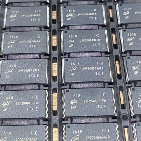
Image for reference only

جزء الشركة المصنعة : جزء الشركة المصنعة

mt29f2f2g08abaeawp:e

الحزمة : الحزمة

TSOP-I-48 (18.4 × 12 مم)

العلامة التجارية : العلامة التجارية
توصيات أخرى قد تكون مهتماً بها.
الوصف

The MT29F2G08ABAEAWP:E is a 2Gb (256MB) SLC NAND Flash from Micron Technology in a 48-pin TSOP-I package. It features an x8 parallel asynchronous interface compliant with ONFI 1.0, with internal 4-bit ECC, 2,048 blocks of 64 pages (2,112 bytes each), page read time of 25 µs, program time of 200 µs, and erase time of 700 µs. The device supports two-plane operations, program/read cache mode, internal data move, and OTP. Operating at 2.7V-3.6V with 35 mA max current, it delivers 100,000 P/E cycle endurance and 10-year data retention. Commercial temperature range: 0°C to +70°C. MSL-3 rated, RoHS compliant, ECCN 3A991.b.1.a.

The MT29F2G08ABAEAWP:E is a 2-gigabit (256MB) single-level cell (SLC) NAND Flash memory device manufactured by Micron Technology. It uses an 8-bit wide (x8) parallel asynchronous interface and is compliant with the Open NAND Flash Interface (ONFI) 1.0 specification. The device is organized as 256M x 8 bits, with 2,048 blocks, each containing 64 pages of 2,112 bytes (2,048 data + 64 spare bytes).

As an SLC NAND device, the MT29F2G08ABAEAWP:E delivers superior endurance and reliability compared to MLC or TLC alternatives, with 100,000 program/erase cycles and 10-year data retention. It features an internal 4-bit ECC engine that can be enabled via GET/SET features or factory-configured to be always active, reducing host controller ECC burden.

The device supports a comprehensive command set including ONFI NAND Flash Protocol basic commands (PAGE READ, PROGRAM PAGE, BLOCK ERASE, READ ID, READ STATUS) and advanced commands (Program Page Cache Mode, Read Page Cache Mode, Internal Data Move with Random Data Input, Two-Plane Commands, Interleaved Die Operations, OTP mode, and Read Unique ID). The two-plane architecture enables simultaneous operations on two planes for increased throughput.

Key performance specifications include a page read time of 25 µs (typical), page program time of 200 µs (typical at 3.3V), and block erase time of 700 µs (typical). The asynchronous I/O interface supports tRC/tWC of 20 ns at 3.3V. Operating voltage range is 2.7V to 3.6V (VCC) with maximum supply current of 35 mA.

The MT29F2G08ABAEAWP:E is packaged in a 48-pin TSOP Type I package with center parting line (CPL), suitable for commercial temperature range (0°C to +70°C). The “:E” suffix in the ordering number indicates the extended marking code format. Note: The -IT:E variant supports industrial temperature range (-40°C to +85°C). Micron has issued a Product Discontinuation Notice (PDN) for some variants of this product family; check with Micron for current lifecycle status.

The MT29F2G08ABAEAWP:E operates as an asynchronous parallel NAND Flash memory device using a highly multiplexed 8-bit bus (I/O[7:0]) to transfer commands, addresses, and data, minimizing pin count while supporting high-density storage.

Command/Address/Data Multiplexing: The five control signals (CE#, CLE, ALE, WE#, RE#) implement the ONFI NAND Flash bus interface protocol. Commands are latched when CLE is HIGH on the rising edge of WE#. Addresses are latched when ALE is HIGH on the rising edge of WE#. Data is transferred bidirectionally on I/O[7:0] under control of WE# (write) and RE# (read). This multiplexed approach reduces the pin count to just 48 pins regardless of density, enabling future density upgrades without PCB redesign.

Page Read Operation: The host issues a PAGE READ command (00h-30h) with the target row address. The device reads the entire page from the NAND array into the page data register in tR (25 µs typical). Once the R/B# signal goes HIGH (ready), the host can sequentially read out data bytes at tRC (20 ns) pace using RE# pulses. Random data access within a page is supported via the RANDOM DATA READ command (05h-E0h).

Page Program Operation: The host issues a PROGRAM PAGE command (80h-10h) with the target address and up to 2,112 bytes of data. Data is loaded into the page data register via WE# pulses, then programmed into the NAND array in tPROG (200 µs typical). The status byte indicates pass/fail upon completion. PROGRAM PAGE CACHE mode allows the next page data to be loaded while the current page is being programmed, overlapping data transfer and programming for higher throughput.

Block Erase Operation: The host issues a BLOCK ERASE command (60h-D0h) with the target block address. The entire 128 KB + 4 KB block is erased in tBERS (700 µs typical), setting all bits to logic 1 (0xFF). The status byte indicates pass/fail.

Two-Plane Operations: The device contains two independent planes of 1,024 blocks each. Two-plane commands allow simultaneous page read, page program, or block erase operations on both planes, effectively doubling throughput for large sequential operations.

Internal ECC: The built-in 4-bit ECC engine can detect and correct up to 4-bit errors per 512-byte sector when enabled. This reduces the minimum host ECC requirement and improves system-level reliability. The spare area mapping changes when internal ECC is active.

Internal Data Move: Data can be copied from one page to another within the same plane without external data transfer, reducing host bandwidth requirements and improving performance for garbage collection and wear leveling operations.

Write Protection: The WP# pin provides hardware write protection, disabling all program and erase operations when held LOW. This prevents accidental data corruption during power transitions.

Bad Block Management: The first block (block address 00h) is guaranteed valid when shipped from the factory with ECC. Additional bad blocks are marked with non-FFh data in the spare area of the first page. The host must implement bad block management to skip or remap detected bad blocks.

دبوس الاسم النوع الوظيفة الافتراضية الوصف
1-6, 22-24, 42-48 نورث كارولاينا No Connect Not internally connected; can be driven or left unconnected for ONFI compatibility
7 R/B# O Ready/Busy Open-drain active-low output; indicates array activity (LOW = busy); requires external pull-up resistor
8 RE# I Read Enable Gates serial data output from the device; active LOW
9 CE# I Chip Enable Activates the device; active LOW; can be de-asserted during program/erase operations
12 VCC P مزود الطاقة Core power supply, 2.7V–3.6V
13 VSS G أرضي Core ground connection
16 CLE I Command Latch Enable When HIGH, data on I/O[7:0] is latched as a command on WE# rising edge
17 ALE I Address Latch Enable When HIGH, data on I/O[7:0] is latched as an address on WE# rising edge
18 WE# I Write Enable Controls write transfers to the device; active LOW
19 WP# I Write Protect Hardware write protect; when LOW, disables all program and erase operations
25-32 I/O[7:0] الإدخال/الإخراج Data Bus Bidirectional data/address/command bus; x8 configuration
التطبيق الوصف
Embedded Boot Storage Reliable SLC NAND for bootloader and firmware storage in embedded systems, industrial controllers, and networking equipment where data integrity is critical
الإلكترونيات الاستهلاكية Mass storage in digital cameras, audio players, and set-top boxes; SLC endurance ensures long product life
Industrial and Automotive -IT:E industrial grade variant (-40°C to +85°C) for PLCs, motor drives, and automotive infotainment; 100K P/E cycles withstand frequent writes
Data Logging High-endurance SLC storage for continuous data logging in medical devices, test equipment, and sensor networks
Density Upgrade Path ONFI-standard pinout allows drop-in upgrade to 4Gb or 8Gb densities in the same 48-pin TSOP footprint without PCB redesign
الطراز الشركة المصنعة التوافق الفرق الرئيسي
MT29F2G08ABAEAWP-IT:E ميكرون Pin-Compatible / Drop-in Industrial temperature range (-40°C to +85°C); same die, wider temp spec; preferred for industrial apps
MT29F2G08ABAEAH4 ميكرون Electrically Equivalent 63-ball VFBGA package instead of TSOP-48; smaller footprint (9×11 mm); same 2Gb SLC capacity
MT29F4G08BABAWP ميكرون متوافق مع الدبوس 4Gb (512MB) density in same 48-pin TSOP; drop-in density upgrade; dual-die stack
MT29F2G16ABAEAWP ميكرون متشابهة وظيفيًا x16 (16-bit) data bus version; same 2Gb density; different I/O organization
S34ML01G2TFI200 إنفينيون (سايبرس) متوافق مع الدبوس 1Gb SLC NAND, TSOP-48, ONFI compatible; alternative supplier; different density
قطع الغيار الموصى بها
4GB eMMC 5.1, HS400, 153-VFBGA, integrated controller, industrial temp

العلامة التجارية:

الحزمة:

153-VFBGA (11.5 x 13.0 x 1.0 mm)
متوفر في المخزون:
11847pcs

دورة الشحن 3 ~ 7 أيام
الحد الأدنى للطلب هو 1

4 جيجا بايت (512 ميجابايت) فلاش SLC NAND، x8، 3.3 فولت، TSOP-48، 2K+64 صفحة، كتلة 128K، 100K دورة، غير متزامن، ONFI 1.0، ECC داخلي 4 بت، 0 ~ 70C

العلامة التجارية:

الحزمة:

48 سنون TSOP من النوع I (12 × 18.4 × 1.0 مم، 0.5 مم، درجة ميل 0.5 مم)
متوفر في المخزون:
1162 قطعة

دورة الشحن 3 ~ 7 أيام
الحد الأدنى للطلب هو 1

4Gbit DDR3L SDRAM، 1866 طن متري/ثانية، 1.35 فولت، 96 كرة FBGA

العلامة التجارية:

الحزمة:

96 كرة FBGA ذات 96 كرة (8 مم × 14 مم × 0.92 مم)
متوفر في المخزون:
3856 قطعة

دورة الشحن 3 ~ 7 أيام
الحد الأدنى للطلب هو 1

ضمان الجودة

تخضع جميع المكونات الإلكترونية التي نحصل عليها من سلاسل التوريد الشريكة لنا لعمليات فحص صارمة للواردات، ومن خلال الاختبارات الدقيقة، نضمن أن كل ما يتم تسليمه للعملاء هو قطع أصلية أصلية وتفي بمتطلبات الجودة، بالإضافة إلى ذلك، نحتفظ بسجلات فحص كاملة لجعل عملية سلسلة التوريد بأكملها واضحة ويمكن تتبعها.

التصديق
لقد حصلنا على عدد من الشهادات الاحترافية وقمنا ببناء مختبر الاختبار الاحترافي الخاص بنا، وهذا يضمن أن كل منتج نقدمه لعملائنا يلبي أعلى متطلبات الجودة، ونجري الاختبارات وفقًا لإجراءات صارمة لضمان جودة المنتج المستقرة والمعايير الدقيقة، ولضمان جودة المنتج المستقرة والمعايير الدقيقة، ولضمان قطع أصلية أصلية، نتعاون أيضًا مع مؤسسات اختبار موثوقة من طرف ثالث لفحص الجودة الصارم، ونولي دائمًا أهمية كبيرة للجودة ونلتزم تمامًا بمعايير الصناعة واللوائح ذات الصلة ومتطلبات ISO 9001: 2015.

الشحن والدفع

تخضع جميع المكونات الإلكترونية التي نحصل عليها من سلاسل التوريد الشريكة لنا لعمليات فحص صارمة للواردات، ومن خلال الاختبارات الدقيقة، نضمن أن كل ما يتم تسليمه للعملاء هو قطع أصلية أصلية وتفي بمتطلبات الجودة، بالإضافة إلى ذلك، نحتفظ بسجلات فحص كاملة لجعل عملية سلسلة التوريد بأكملها واضحة ويمكن تتبعها.

التصديق
لقد حصلنا على عدد من الشهادات الاحترافية وقمنا ببناء مختبر الاختبار الاحترافي الخاص بنا، وهذا يضمن أن كل منتج نقدمه لعملائنا يلبي أعلى متطلبات الجودة، ونجري الاختبارات وفقًا لإجراءات صارمة لضمان جودة المنتج المستقرة والمعايير الدقيقة، ولضمان جودة المنتج المستقرة والمعايير الدقيقة، ولضمان قطع أصلية أصلية، نتعاون أيضًا مع مؤسسات اختبار موثوقة من طرف ثالث لفحص الجودة الصارم، ونولي دائمًا أهمية كبيرة للجودة ونلتزم تمامًا بمعايير الصناعة واللوائح ذات الصلة ومتطلبات ISO 9001: 2015.

الخدمة والتغليف

تخضع جميع المكونات الإلكترونية التي نحصل عليها من سلاسل التوريد الشريكة لنا لعمليات فحص صارمة للواردات، ومن خلال الاختبارات الدقيقة، نضمن أن كل ما يتم تسليمه للعملاء هو قطع أصلية أصلية وتفي بمتطلبات الجودة، بالإضافة إلى ذلك، نحتفظ بسجلات فحص كاملة لجعل عملية سلسلة التوريد بأكملها واضحة ويمكن تتبعها.

التصديق
لقد حصلنا على عدد من الشهادات الاحترافية وقمنا ببناء مختبر الاختبار الاحترافي الخاص بنا، وهذا يضمن أن كل منتج نقدمه لعملائنا يلبي أعلى متطلبات الجودة، ونجري الاختبارات وفقًا لإجراءات صارمة لضمان جودة المنتج المستقرة والمعايير الدقيقة، ولضمان جودة المنتج المستقرة والمعايير الدقيقة، ولضمان قطع أصلية أصلية، نتعاون أيضًا مع مؤسسات اختبار موثوقة من طرف ثالث لفحص الجودة الصارم، ونولي دائمًا أهمية كبيرة للجودة ونلتزم تمامًا بمعايير الصناعة واللوائح ذات الصلة ومتطلبات ISO 9001: 2015.



