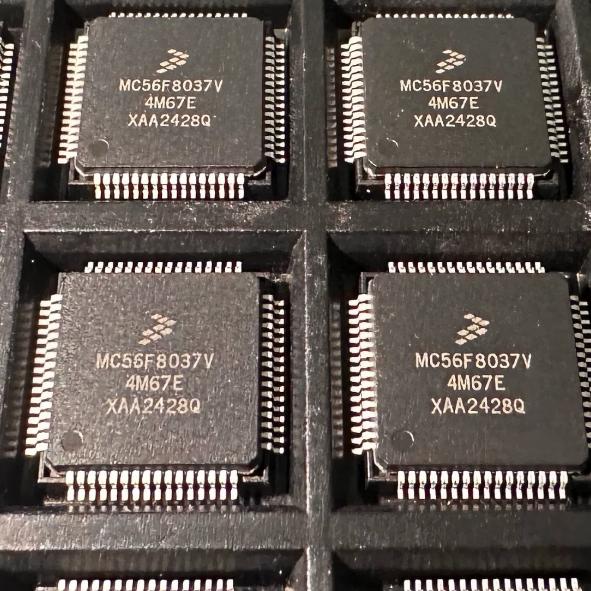
The MC56F8037VLH from NXP Semiconductors (formerly Freescale) is a 16-bit Digital Signal Controller (DSC) that combines digital signal processing and microcontroller functionalities on a single chip. It is based on the 56800E core, a dual Harvard-style architecture with three parallel execution units that can perform up to six operations per instruction cycle.
The 56800E core operates at 32 MHz, delivering 32 MIPS performance. It features a single-cycle 16×16-bit parallel MAC (Multiply-Accumulate), four 36-bit accumulators with extension bits, a 32-bit ALU with multi-bit shifter, hardware DO and REP loops, and parallel instruction set with unique DSP addressing modes. The MCU-style programming model and optimized instruction set support efficient C compiler output for rapid development.
Memory includes 64 KB (32K x 16) program Flash with page erase (512 bytes/page) and security/protection features, plus 8 KB (4K x 16) unified data/program RAM. The dual Harvard architecture allows up to three simultaneous memory accesses per instruction cycle. EEPROM emulation is possible using the Flash.
The 6-channel PWM module operates at up to 96 MHz clock with 15-bit resolution, supporting both center-aligned and edge-aligned modes. Four programmable fault inputs with digital filters provide protection. The PWM outputs can be sourced from the PWM generator, external GPIO, internal timers, analog comparators, or ADC limit comparisons.
Two independent 12-bit ADCs provide 2 x 8 channels with simultaneous and sequential conversion support, synchronized by PWM and timer modules at up to 2.67 MSPS. Two 12-bit DACs feature 2 us settling time and automatic waveform generation (square, triangle, sawtooth).
Communication peripherals include two QSCI (UART with LIN slave), two QSPI, one I2C (400 kbps), and one MSCAN (CAN 2.0A/B, up to 1 Mbps, 5 RX + 3 TX buffers). Two Quad Timer modules provide eight 16-bit counter/timers with 12 operating modes each.
The MC56F8037VLH includes 53 GPIO pins with 5 V tolerance, JTAG/OnCE debug interface, on-chip regulators, PLL, internal relaxation oscillator, and power management (Wait and Stop modes). The 64-LQFP package measures 10 x 10 mm.
Note: NXP designates the 56F803X family as “Not Recommended for New Designs” (NRND). The product is included in NXP’s product longevity program with assured supply for a minimum of 10 years after launch. Designers should consider the MC56F837xx or Kinetis KV series for new designs.





 English
  简体中文
简体中文  Español
  العربية




