首页 > 集成电路 IC > BSS123-7-F

BSS123-7-F


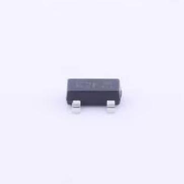
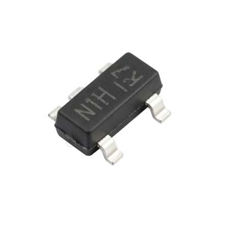
N 沟道增强型 MOSFET,100V,170 mA,6 Ω RDS(导通),SOT-23-3,AEC-Q101

207116

有效库存
转到查询

Image for reference only

制造商零件:

BSS123-7-F

包装:

SOT-23-3(2.9 x 1.3 毫米)

品牌:
产品类别:
您可能感兴趣的其他建议.
说明

BSS123-7-F 是 Diodes Incorporated 推出的一款 N 沟道增强型沟槽 MOSFET,具有 100 V 漏极-源极电压、170 mA 连续漏极电流、VGS = 10 V 时 6 Ω RDS(on)和最大 2.0 V VGS(th)。该器件具有 60 pF 输入电容、300 mW 功耗和 AEC-Q101 认证,是低端负载开关、逻辑电平转换和通用数字控制的理想之选。该器件采用 SOT-23-3(2.9 x 1.3 mm)封装,符合 MSL-1 评级和无铅标准,工作在 -55°C 至 +150°C 的结温范围内。以卷带(3000 个/卷)供应。.

The BSS123-7-F is an N-channel enhancement mode MOSFET manufactured by Diodes Incorporated, utilizing proprietary high-density trench technology. It features a drain-source breakdown voltage (VDSS) of 100 V, continuous drain current (ID) of 170 mA at 25°C ambient, and on-resistance (RDS(on)) of 6 Ω maximum at VGS = 10 V and ID = 170 mA. The gate-source threshold voltage (VGS(th)) is 2.0 V maximum at ID = 1 mA.

Key electrical characteristics include a maximum gate-source voltage of ±20 V, input capacitance (Ciss) of 60 pF maximum at VDS = 25 V, and power dissipation of 300 mW at 25°C ambient. The device operates over a junction temperature range of -55°C to +150°C.

The BSS123-7-F is packaged in the industry-standard SOT-23-3 (TO-236-3, SC-59) package with dimensions of 2.9 x 1.3 x 1.0 mm. It features a matte tin finish annealed over alloy 42 lead frame, UL94V-0 flame-rated molded plastic case, and is MSL-1 rated (unlimited floor life). The -7 suffix denotes tape and reel packaging (3000 units per reel), and the -F suffix indicates green (Pb-free) compliance. The device is also AEC-Q101 qualified for automotive applications.

The low gate threshold voltage, low input capacitance, and fast switching speed make this MOSFET ideal for low-voltage and low-current switching applications such as level shifting, load switching, and general-purpose digital control.

The BSS123-7-F is an N-channel enhancement mode MOSFET that operates by modulating the conductivity of a channel between source and drain using an electric field applied to the gate terminal.

Enhancement Mode Operation: With no gate-source voltage applied (VGS = 0 V), the MOSFET is in the off state. There is no conductive channel between drain and source, and only a tiny leakage current (IDSS) flows. This is the normally-off characteristic of enhancement mode devices.

Channel Formation: When a positive gate-source voltage exceeding the threshold voltage (VGS(th)) is applied, the electric field attracts electrons to the semiconductor surface beneath the gate oxide, forming an inversion layer (conducting channel) between source and drain. For the BSS123-7-F, VGS(th) is typically around 1.0-1.4 V, with a maximum of 2.0 V at ID = 1 mA.

Ohmic (Linear) Region: At low VDS, the drain current is approximately proportional to VDS, and the channel behaves like a resistor with value RDS(on). The RDS(on) is 6 Ω maximum at VGS = 10 V. Higher VGS increases the channel charge density, reducing RDS(on) and increasing drain current capability.

Saturation Region: At higher VDS, the channel pinches off near the drain end, and the drain current becomes relatively independent of VDS, limited by the gate voltage. The device acts as a current source in this region.

Switching Behavior: The MOSFET is voltage-driven and requires virtually no steady-state gate current (only the gate leakage current, typically less than 100 nA). The switching speed is determined by the time required to charge and discharge the input capacitance (Ciss = 60 pF max) through the gate driver impedance. The low Ciss enables fast turn-on and turn-off transitions, making the device suitable for high-frequency switching applications.

Trench Technology: The BSS123-7-F uses trench MOSFET technology, where the gate structure is formed vertically in a trench etched into the silicon. This approach reduces cell size and increases channel density per unit area, achieving lower RDS(on) for a given die size compared to planar MOSFET construction.

针脚 名称 类型 默认功能 说明
1 大门 I Gate Control Input Voltage-controlled input; drives channel formation between drain and source; high impedance DC input
2 资料来源 G Source Terminal Current source terminal; typically connected to ground in low-side switch configuration
3 排水 O Drain Terminal Current drain terminal; connects to load in switching applications
应用 说明
低侧负载开关 Switching resistive or inductive loads such as LEDs, relays, and small motors with gate drive from 3.3V or 5V logic
Logic Level Shifting Bi-directional or unidirectional voltage level translation between 3.3V and 5V logic domains in mixed-voltage systems
Battery-Powered Device Control Power gating and sleep-mode control in portable devices; low gate threshold enables operation from single-cell lithium supplies
Automotive Body Electronics AEC-Q101 qualified switching for interior lighting, door lock actuators, and sensor signal conditioning in automotive body control modules
General-Purpose Digital Control Microcontroller GPIO expansion for driving loads beyond direct GPIO current capability; 100V rating provides margin for inductive kickback
模型 制造商 兼容性 主要区别
BSS123 恩智浦/各种 针脚兼容 Industry-standard equivalent; same pinout and similar specs; verify RDS(on) and VGS(th) matching for specific manufacturer
2N7002 各种 针脚兼容 60V, 115 mA, 1.2-2.8 Ω RDS(on); lower voltage, lower RDS(on), different VGS(th) range; most common small-signal MOSFET alternative
MMBF170 onsemi 针脚兼容 60V, 500 mA; higher current rating, lower RDS(on); different threshold voltage characteristics
BSS138 Diodes Incorporated / Various 针脚兼容 50V, 220 mA, 3.5 Ω RDS(on); lower voltage, lower RDS(on), popular for level shifting
DMN2075U 二极管公司 功能相似 20V, 750 mA, 0.75 Ω; much lower voltage but higher current and lower RDS(on); SOT-23; for low-voltage applications
推荐部件
PNP BJT、60V、600mA、100 分钟 hFE、200MHz fT、SOT-23-3、AEC-Q101、低 VCE(饱和)、绿色器件

品牌:

封装:

SOT-23-3(TO-236-3,SC-59),2.9 x 1.3 x 1.0 毫米
有库存:
6952 件

货运周期:3~7 天
最低订购量为 1

转到查询
100V N 沟道 MOSFET,1.6A,220mOhm@10V,8.3nC Qg,SOT-23-3 T/R,低成本负载开关

品牌:

封装:

SOT-23-3(2.9 x 1.3 x 0.98 毫米,鸥翼型)
有库存:
35443 件

货运周期:3~7 天
最低订购量为 1

转到查询
-20V P-ch MOSFET、-10A、13mOhm@-10V、56.9nC Qg、SO-8、AEC-Q101、负载开关

品牌:

封装:

SO-8 / SOP-8(5.0 x 4.0 x 1.5 毫米,1.27 毫米间距,鸥翼型)
有库存:
4342 件

货运周期:3~7 天
最低订购量为 1

转到查询
30V 单向 TVS、225W Ppp、48.4V clamp@4.65A、33.3-36.8V VBR、PowerDI 123、AEC-Q101

品牌:

封装:

PowerDI 123(3.7 x 2.8 x 1.78 毫米,2 引脚,SMD)
有库存:
4734 件

货运周期:3~7 天
最低订购量为 1

转到查询
20V N 沟道 MOSFET、12A、8mΩ@10V、9mΩ@4.5V、SO-8、2W、DC-DC/负载开关

品牌:

封装:

SO-8(5.0 x 4.0 x 1.5 毫米,1.27 毫米间距,鸥翼型)
有库存:
1889 件

货运周期:3~7 天
最低订购量为 1

转到查询
60V N 沟道 MOSFET,320mA,1.3Ω@4V,ESD 保护栅极,X1-DFN1006(0.6mm²),0.45nC Qg

品牌:

封装:

X1-DFN1006-3(1.0 x 0.6 x 0.47 毫米,0.5 毫米间距,底部端子)
有库存:
17922 件

货运周期:3~7 天
最低订购量为 1

转到查询
质量保证

我们从合作供应链采购的所有电子元件都经过严格的进货检验。通过仔细的测试,我们确保交付给客户的所有产品都是原装正品,符合质量要求。此外,我们还保存完整的检验记录,使整个供应链流程清晰可查。.

认证
我们获得了多项专业认证,并建立了自己的专业检测实验室,确保交付给客户的每一件产品都符合最高质量要求。我们严格按照流程进行检测,确保产品质量稳定、参数准确。为保证原装正品,我们还与可靠的第三方检测机构合作,进行严格的质量检测。我们始终高度重视质量,完全符合行业标准、相关法规和 ISO 9001:2015 的要求。.

发货与付款

我们从合作供应链采购的所有电子元件都经过严格的进货检验。通过仔细的测试,我们确保交付给客户的所有产品都是原装正品,符合质量要求。此外,我们还保存完整的检验记录,使整个供应链流程清晰可查。.

认证
我们获得了多项专业认证,并建立了自己的专业检测实验室,确保交付给客户的每一件产品都符合最高质量要求。我们严格按照流程进行检测,确保产品质量稳定、参数准确。为保证原装正品,我们还与可靠的第三方检测机构合作,进行严格的质量检测。我们始终高度重视质量,完全符合行业标准、相关法规和 ISO 9001:2015 的要求。.

服务与包装

我们从合作供应链采购的所有电子元件都经过严格的进货检验。通过仔细的测试,我们确保交付给客户的所有产品都是原装正品,符合质量要求。此外,我们还保存完整的检验记录,使整个供应链流程清晰可查。.

认证
我们获得了多项专业认证,并建立了自己的专业检测实验室,确保交付给客户的每一件产品都符合最高质量要求。我们严格按照流程进行检测,确保产品质量稳定、参数准确。为保证原装正品,我们还与可靠的第三方检测机构合作,进行严格的质量检测。我们始终高度重视质量,完全符合行业标准、相关法规和 ISO 9001:2015 的要求。.