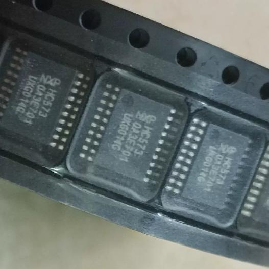
The 74HC573PW from Nexperia is an octal (8-bit) D-type transparent latch with 3-state outputs, housed in a 20-pin TSSOP package. It is one of the most widely used bus latch devices in digital system design, particularly for microprocessor and microcontroller address/data bus demultiplexing.
The 74HC573 is functionally identical to the 74HC373, but with a different pinout that places all data inputs on one side of the package and all outputs on the opposite side. This flow-through pinout dramatically simplifies PCB layout for bus-oriented designs, where the data bus flows from left to right (or top to bottom) through the latch. The 74HC373, by contrast, has inputs and outputs interleaved, making bus routing more complex.
The device provides two control functions: latch enable (LE) and output enable (OE). The LE pin controls whether the latches are transparent (passing input data to outputs) or holding (latching the last data). The OE pin controls whether the outputs are active (driving the bus) or in the high-impedance state (disconnected from the bus). These two controls operate independently: OE affects only the output buffers, not the internal latch state, so the latched data is preserved even when the outputs are disabled.
Transparent Latch Operation: When LE is HIGH, each D input passes directly through its respective latch to the corresponding Q output. The latch is said to be ‘transparent’ because the output follows the input with only the propagation delay (approximately 14ns at VCC=4.5V). This mode is used during the time when the microprocessor is driving the address/data bus with valid data. When LE transitions from HIGH to LOW, the data present at the D inputs at the moment of the falling edge is captured (latched) and held at the Q outputs. The latch then becomes opaque – changes on the D inputs no longer affect the Q outputs until LE goes HIGH again.
3-State Output Control: The OE pin controls the output buffers independently of the latch state. When OE is LOW (active), the outputs drive the bus with the latched data. When OE is HIGH, all outputs enter the high-impedance (Hi-Z) state, effectively disconnecting the device from the bus. This allows multiple devices to share a common output bus without contention. The internal latch continues to hold its data even when the outputs are disabled, so the data is immediately available when OE goes LOW again.
Microprocessor Bus Demultiplexing: The primary application of the 74HC573 is demultiplexing the combined address/data bus used by many microprocessors and microcontrollers. In these systems, the same physical pins carry both address and data information on different clock phases. The 74HC573 captures the address during the address phase (LE=HIGH, then LE goes LOW to latch), and the latched address remains stable on the outputs while the bus transitions to the data phase. This allows the system to use the address for memory decoding while the data bus is free for read/write operations.
The 74HC573 is also commonly used as an output port expander. A microcontroller writes data to the latch by driving the D inputs and pulsing LE. The latched data then drives external peripherals (LEDs, relays, displays) independently of the microcontroller bus state. The OE pin can be used to enable/disable the port outputs as needed.
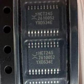
The 74HC variant operates over the full 2.0V to 6.0V supply range with CMOS input levels, while the 74HCT variant operates at 4.5V to 5.5V with TTL-compatible input levels. The HCT variant is preferred when interfacing with 5V TTL or CMOS logic, while the HC variant is used for lower-voltage applications.
Input clamp diodes on all inputs allow interfacing with voltages in excess of VCC through current-limiting resistors. This feature is useful in mixed-voltage systems where input signals may come from a higher-voltage domain. The latch-up performance exceeds 100mA per JESD 78 Class II Level B, ensuring reliable operation in harsh electrical environments.





 English
  简体中文
简体中文  Español
  العربية




