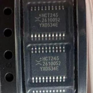
74HCT245PW


Octal bus transceiver, 3-state, non-inverting, TTL-input, 4.5-5.5V, 10ns prop delay, TSSOP-20, -40~125C

550000

Effective Inventory
Go to Inquiry

Image for reference only

Manufacturer Part:

74HCT245PW

Package:

TSSOP-20 (SOT360-1) (6.50 x 6.40 x 1.10 mm, 0.65mm pitch)

Brand:
Product Categories:
Other recommendations you may be interested in.
Description

The 74HCT245PW from Nexperia (formerly NXP/Philips) is an octal bus transceiver with non-inverting 3-state outputs in a 20-pin TSSOP (SOT360-1) package (6.50 x 6.40 x 1.10 mm). It is designed for asynchronous bidirectional communication between data buses. The device features an output enable input (OE, active LOW) for easy cascading and a direction control input (DIR) for send/receive selection. When OE is HIGH, both A and B outputs are in the high-impedance state, effectively isolating the buses. When OE is LOW, the DIR pin determines data flow direction: DIR=LOW sends data from A to B; DIR=HIGH sends data from B to A. The 74HCT245 has TTL-compatible input levels (VIH min 2.0V, VIL max 0.8V at VCC=4.5V) and CMOS-level outputs. Supply voltage: 4.5V to 5.5V. Propagation delay: 10ns typical at VCC=5V. Output drive: plus/minus 6mA at 5V. Low power consumption: 80uA max ICC. Low input current: 1uA max. ESD protection: HBM exceeds 2000V, MM exceeds 200V. Latch-up performance exceeds 100mA per JESD78 Class II. Operating temperature: -40C to +125C. Active product, RoHS compliant, EAR99. The PW package is pin-compatible with TI’s SN74HCT245PW and other manufacturers’ 74HCT245 TSSOP-20 variants.

The 74HCT245PW from Nexperia is an octal (8-bit) bidirectional bus transceiver with non-inverting 3-state outputs, designed for asynchronous two-way communication between data buses. It is one of the most widely used standard logic devices in digital system design, serving as the primary interface between processors, memory, and peripheral devices on shared bus architectures.

The 74HCT245 belongs to the 74HC/HCT family of high-speed silicon-gate CMOS devices. The HCT variant features TTL-compatible input voltage levels (VIH minimum 2.0V at VCC=4.5V), making it ideal for interfacing between TTL and CMOS logic families. This compatibility allows the 74HCT245 to accept signals from TTL-level microprocessors, ASICs, and FPGAs while driving CMOS-level loads, without requiring external level-shifting circuitry.

The device provides two control inputs that manage bus operation. The output enable (OE) input, active LOW, controls whether the outputs are active or in the high-impedance state. When OE is HIGH, all outputs assume a high-impedance (3-state) condition, effectively disconnecting the device from both buses. This allows multiple 74HCT245 devices to share the same bus in a wired-OR configuration without bus contention. The direction (DIR) input determines the data flow direction: when DIR is LOW, data flows from the A bus to the B bus; when DIR is HIGH, data flows from the B bus to the A bus.

The 3-state output capability is essential for bus-oriented systems. In a typical microprocessor system, multiple devices (memory, I/O controllers, DMA controllers) share a common data bus. Only one device can drive the bus at any given time. The 3-state outputs of the 74HCT245 allow a device to be electrically disconnected from the bus when it is not actively driving data, preventing bus contention and signal corruption.

The non-inverting characteristic means that the data passes through the transceiver without inversion: a HIGH on the input appears as a HIGH on the output. This simplifies system design by eliminating the need to account for signal inversion in the bus interface logic. For applications requiring inversion, the 74HCT640 (inverting version) is available in the same pinout.

The propagation delay of 10ns typical at VCC=5V makes the 74HCT245 suitable for moderate-speed bus systems. The output drive capability of plus/minus 6mA at 5V can directly drive bus lines or up to 15 LSTTL loads, providing adequate fan-out for most applications. The balanced output design ensures symmetrical rise and fall times, minimizing signal skew on the bus.

The TSSOP-20 (PW) package offers a compact footprint compared to the traditional SOIC-20 (D) package, making it suitable for space-constrained designs such as portable equipment and dense circuit boards. The 0.65mm pin pitch is compatible with standard PCB manufacturing processes.

The device includes positive input clamp diodes on all inputs, which limit negative voltage excursions below GND. This allows the use of current-limiting resistors to interface inputs to voltages in excess of VCC, enabling direct connection to higher-voltage bus signals without damage. The latch-up performance exceeds 100mA per JESD78 Class II, ensuring robust operation in electrically noisy environments.

The 74HCT245 is part of a large family of bus transceivers with various configurations. Related devices include the 74HC245 (CMOS input levels, wider VCC range of 2-6V), 74LVC245 (lower voltage, 1.65-3.6V), 74LVT245 (2.7-3.6V with higher drive), and 74ABT245 (5V with very high drive). The 74HCT245 occupies the sweet spot for 5V systems that need TTL-compatible inputs with CMOS-level outputs.

The 74HCT245PW operates as an 8-bit bidirectional bus transceiver using two sets of 3-state buffers controlled by OE and DIR inputs.

Internal Architecture: The device contains 16 3-state buffers organized as 8 pairs. Each pair connects one A-bus line to one B-bus line. One buffer in each pair drives from A to B, and the other drives from B to A. The OE and DIR control inputs select which set of buffers is enabled, or whether all buffers are disabled.

Control Logic: The control logic decodes the OE and DIR inputs as follows:
1. OE=HIGH, DIR=X: All outputs are in the high-impedance (3-state) condition. Both the A and B bus pins are effectively disconnected from the internal circuitry. This allows other devices to drive the bus without contention.
2. OE=LOW, DIR=LOW: The A-to-B buffers are enabled. Data present on the A0-A7 pins is transmitted through the non-inverting buffers to the B0-B7 pins. The A bus pins are configured as inputs and the B bus pins are outputs.
3. OE=LOW, DIR=HIGH: The B-to-A buffers are enabled. Data present on the B0-B7 pins is transmitted through the non-inverting buffers to the A0-A7 pins. The B bus pins are configured as inputs and the A bus pins are outputs.

3-State Output Stage: Each output buffer has a 3-state output stage consisting of a PMOS pull-up transistor and an NMOS pull-down transistor in a push-pull configuration, plus a disable circuit that turns off both transistors. When the output is active, one transistor is on and the other is off, driving the output HIGH or LOW. When the output is in the high-impedance state, both transistors are off, and the output pin presents a very high impedance to the bus (only leakage current flows). The output enable circuitry ensures that the disable transition happens cleanly, with the output going to high-impedance before any other device begins driving the bus.

TTL-Compatible Input Stage (HCT): The HCT variant uses a modified input stage that responds to TTL voltage levels. In standard CMOS (HC), the input switching threshold is approximately VCC/2 (2.5V at 5V). In the HCT variant, the switching threshold is shifted lower to approximately 1.4V, matching the TTL specification. This is achieved by adjusting the P/N ratio of the input inverter and adding a level-shifting circuit. The HCT input accepts VIH as low as 2.0V (vs. 3.5V for HC at 5V) and VIL as high as 0.8V, directly compatible with TTL output specifications (VOH min 2.4V, VOL max 0.4V).

Bus Contention Prevention: In systems with multiple bus transceivers, the OE signal is used to ensure that only one device drives the bus at any time. The bus controller typically uses address decoding logic to generate individual OE signals for each transceiver. The turn-off time of the 74HCT245 (typically 10ns) ensures that the current driver releases the bus quickly enough for the next driver to take over without a significant dead time.

Power Dissipation: The static power consumption of the HCT variant is higher than the HC variant due to the additional DC current drawn by the TTL-compatible input stage when driven with TTL-level signals. The additional supply current is approximately 400uA per input at VCC=4.5V to 5.5V when driven with VIH=VCC-2.1V. The dynamic power consumption is determined by the load capacitance and switching frequency: PD = CPD x VCC squared x fi x N, where CPD is the power dissipation capacitance per buffer.

Pin Name Type Description
1 DIR Input Direction control; LOW = data flows A to B (A inputs, B outputs); HIGH = data flows B to A (B inputs, A outputs); must be set before OE is asserted to avoid bus glitches; input levels: TTL-compatible (VIH min 2.0V, VIL max 0.8V at VCC=4.5V)
2 A0 I/O Bus A data line 0; input when DIR=LOW (A-to-B mode); output when DIR=HIGH (B-to-A mode); high-impedance when OE=HIGH
3 A1 I/O Bus A data line 1
4 A2 I/O Bus A data line 2
5 A3 I/O Bus A data line 3
6 A4 I/O Bus A data line 4
7 A5 I/O Bus A data line 5
8 A6 I/O Bus A data line 6
9 A7 I/O Bus A data line 7
10 GND Ground Ground reference (0V); connect to PCB ground plane; all output currents return through this pin
11 B7 I/O Bus B data line 7; output when DIR=LOW (A-to-B mode); input when DIR=HIGH (B-to-A mode); high-impedance when OE=HIGH
12 B6 I/O Bus B data line 6
13 B5 I/O Bus B data line 5
14 B4 I/O Bus B data line 4
15 B3 I/O Bus B data line 3
16 B2 I/O Bus B data line 2
17 B1 I/O Bus B data line 1
18 B0 I/O Bus B data line 0
19 OE Input Output enable; active LOW; LOW = outputs enabled (data flows per DIR); HIGH = all outputs in high-impedance state (bus isolated); TTL-compatible input levels; typically driven by address decode logic
20 VCC Power Supply voltage; 4.5V to 5.5V (HCT); decouple with 0.1uF ceramic capacitor to GND close to the device; maximum ICC = 80uA (static)
Application Description
Microprocessor Bus Interface Buffer data bus between CPU and memory/peripherals; TTL-compatible inputs accept 3.3V or 5V logic from microprocessors; 3-state outputs allow bus sharing among multiple devices; DIR pin controlled by read/write signal; OE pin controlled by chip select decoding; 6mA drive sufficient for typical backplane loads
Level Translation (5V to 3.3V) Interface 5V CMOS bus to 3.3V logic; TTL-compatible inputs on HCT variant accept 3.3V logic HIGH (VOH ~2.4V) as valid VIH; 5V VCC provides 5V output swing to drive 5V loads; simplifies mixed-voltage system design without dedicated level shifters
I/O Port Expansion Add bidirectional I/O ports to microcontrollers; one 74HCT245 provides 8 bits of bidirectional I/O with only 2 control lines (DIR and OE); 3-state outputs prevent bus contention when port is not being accessed; multiple devices can share the same bus with individual OE signals
Bus Isolation and Hot-Swap Isolate boards or subsystems from the shared bus; OE=HIGH disconnects board from bus, allowing safe insertion/removal; clamp diodes on inputs protect against negative voltage transients during hot-swap events; used in backplane systems and modular chassis
Memory Bank Switching Enable switching between multiple memory banks sharing the same data bus; each bank uses a 74HCT245 with individual OE control; only one bank is active at a time, preventing bus contention; DIR line always set for memory read direction (B-to-A) or write direction (A-to-B)
Model Manufacturer Compatibility Key Difference
SN74HCT245PW TI Drop-In Compatible Same function, same TSSOP-20 pinout; TI variant with identical specifications; also available in SOIC-20, SSOP-20, VSSOP-20; active product; fully interchangeable with Nexperia 74HCT245PW
74HC245PW Nexperia Same, CMOS Input Same pinout and function; HC variant with CMOS input levels (VIH = 0.7xVCC); wider VCC range 2.0-6.0V; use when interfacing CMOS-level signals; lower additional supply current at TTL input levels
74LVC245APW Nexperia Lower Voltage Low-voltage variant; 1.65-3.6V supply; 24mA output drive; 5V tolerant inputs; same TSSOP-20 pinout; use for 3.3V and lower voltage systems
74HCT640PW Nexperia Inverting Version Inverting bus transceiver; same pinout; data is inverted when passing through; use when signal inversion is needed in the bus interface
74HCT245D Nexperia Same in SOIC-20 Same function in SOIC-20 (SOT163-1) package; wider body (7.5mm); easier hand soldering; same pinout; use when TSSOP footprint is not required
Recommend Parts
SPDT analog switch, 6Ω RON, 1.65-5.5V, 300MHz BW, BBM, TSSOP6

Brand:

Package:

TSSOP6 / SOT363-2 (2.1 x 1.25 x 0.95mm)
In stock:
14113pcs

Cargo cycle: 3~7 Days
The minimum order is 1

Go to Inquiry
Dual common-cathode Schottky, 30V, 200mA, 240mV@1mA, 5ns trr, SOT-23, AEC-Q101

Brand:

Package:

SOT-23 / TO-236AB (2.9 x 1.3 x 1.0 mm, 1.9mm pitch)
In stock:
362417pcs

Cargo cycle: 3~7 Days
The minimum order is 1

Go to Inquiry
PNP 40V 200mA, hFE 100-300, fT 250MHz, SOT-23, complementary to MMBT3904, general-purpose switching

Brand:

Package:

SOT-23 (TO-236) (2.9 x 1.3 x 1.0 mm, 1.9mm pitch)
In stock:
80000pcs

Cargo cycle: 3~7 Days
The minimum order is 1

Go to Inquiry
N-ch small-signal MOSFET, 50V/173mA, 15 ohm RDS(on)@10V, logic-level, TrenchMOS, SOT-23, -65~150C

Brand:

Package:

SOT-23 (TO-236AB) (2.9 x 1.3 x 1.0 mm, 1.9mm pitch)
In stock:
0pcs

Cargo cycle: 3~7 Days
The minimum order is 1

Go to Inquiry
Octal D-type transparent latch, 3-state outputs, LE and OE control, 2-6V, TSSOP-20, -40~125C, I/O on opposite sides for bus interfacing

Brand:

Package:

TSSOP-20 (SOT360-1) (6.4 x 4.4 x 1.2 mm)
In stock:
24829pcs

Cargo cycle: 3~7 Days
The minimum order is 1

Go to Inquiry
3-to-8 decoder/demux, active-HIGH outputs, 3 enable inputs, 2-6V, TSSOP-16, -40~125C, similar to 74HC138 but non-inverting

Brand:

Package:

TSSOP-16 (SOT403-1) (5.0 x 4.4 x 1.2 mm)
In stock:
85000pcs

Cargo cycle: 3~7 Days
The minimum order is 1

Go to Inquiry
Quality Assurance

All electronic components we source from our partnered supply chains go through strict incoming inspections.Through careful testing, we ensure everything delivered to customers is genuine original parts and meets quality requirements.In addition, we keep complete inspection records to make the entire supply chain process clear and traceable.

Certification
We have obtained a number of professional certifications and built our own professional testing laboratory.This ensures that every product we deliver to our customers meets the highest quality requirements.We conduct tests in strict accordance with procedures to ensure stable product quality and accurate parameters.To guarantee genuine original parts, we also cooperate with reliable third-party testing institutions for strict quality inspection.We always attach great importance to quality and fully comply with industry standards, relevant regulations, and ISO 9001:2015 requirements.

Shipping & Payment

All electronic components we source from our partnered supply chains go through strict incoming inspections.Through careful testing, we ensure everything delivered to customers is genuine original parts and meets quality requirements.In addition, we keep complete inspection records to make the entire supply chain process clear and traceable.

Certification
We have obtained a number of professional certifications and built our own professional testing laboratory.This ensures that every product we deliver to our customers meets the highest quality requirements.We conduct tests in strict accordance with procedures to ensure stable product quality and accurate parameters.To guarantee genuine original parts, we also cooperate with reliable third-party testing institutions for strict quality inspection.We always attach great importance to quality and fully comply with industry standards, relevant regulations, and ISO 9001:2015 requirements.

Service & Packaging

All electronic components we source from our partnered supply chains go through strict incoming inspections.Through careful testing, we ensure everything delivered to customers is genuine original parts and meets quality requirements.In addition, we keep complete inspection records to make the entire supply chain process clear and traceable.

Certification
We have obtained a number of professional certifications and built our own professional testing laboratory.This ensures that every product we deliver to our customers meets the highest quality requirements.We conduct tests in strict accordance with procedures to ensure stable product quality and accurate parameters.To guarantee genuine original parts, we also cooperate with reliable third-party testing institutions for strict quality inspection.We always attach great importance to quality and fully comply with industry standards, relevant regulations, and ISO 9001:2015 requirements.