TIP122


NPN 达林顿功率晶体管,100V,5A,hFE 1000min,TO-220,VCE(饱和)2V@3A,与 TIP127 互补

205384

有效库存
转到查询

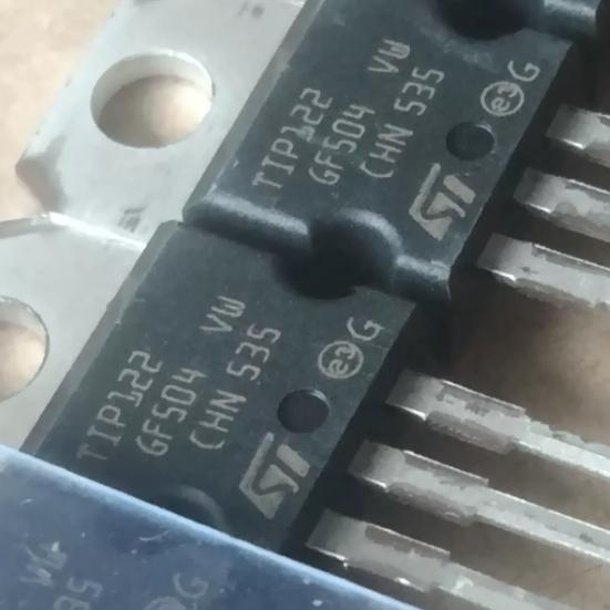
Image for reference only

制造商零件:

TIP122

包装:

TO-220AB(3 引脚 + 凸片)(10.4 x 4.6 x 9.15 毫米)

品牌:
您可能感兴趣的其他建议.
说明

The TIP122 from onsemi is an NPN Darlington bipolar power transistor in a TO-220AB package, rated for 100V VCEO and 5A continuous collector current (8A peak). The Darlington configuration provides extremely high DC current gain (hFE minimum 1000 at IC=3A, typical 2500 at IC=4A), allowing it to be driven directly from low-power logic outputs including microcontrollers and TTL circuits. VCE(sat) is 2.0V max at IC=3A/IB=12mA and 4.0V max at IC=5A/IB=20mA. The device features monolithic construction with built-in base-emitter shunt resistors for improved stability and leakage control. Maximum power dissipation: 65W at Tc=25C with heatsink (2W without heatsink at Ta=25C). Junction temperature range: -65C to 150C. Complementary PNP device: TIP127. The TIP122 is part of the TIP120/121/122 NPN family (60V/80V/100V respectively) with corresponding TIP125/126/127 PNP complements. Active product, Pb-free available, EAR99.

The TIP122 from onsemi (formerly Motorola/ON Semiconductor) is a silicon NPN Darlington power transistor designed for general-purpose amplifier and low-speed switching applications. Housed in the ubiquitous TO-220AB through-hole package, the TIP122 is one of the most widely used Darlington transistors in hobbyist, educational, and industrial electronics.

The Darlington configuration integrates two NPN transistors on a single monolithic die, with the collector of the first transistor connected to the collector of the second, and the emitter of the first driving the base of the second. This cascade connection multiplies the current gains of the two individual transistors, resulting in an overall hFE (DC current gain) of at least 1000 and typically 2500 at IC=4A. The practical implication is significant: a base current of only 2-5mA from a microcontroller GPIO pin can control loads of several amps, making the TIP122 an ideal interface between low-power digital logic and high-power analog loads.

The built-in base-emitter shunt resistors serve two critical purposes: (1) they provide a discharge path for stored charge in the base-emitter junctions when the transistor is turning off, improving switching speed and reducing storage time; and (2) they divert leakage current away from the base-emitter junctions at high temperatures, preventing thermal runaway and false turn-on that can occur with high-gain Darlington devices. Without these shunt resistors, the high gain of the Darlington pair would make the device extremely sensitive to temperature-induced leakage currents.

The TIP122 is part of a voltage-graded family: TIP120 (60V VCEO), TIP121 (80V VCEO), and TIP122 (100V VCEO), all sharing identical electrical characteristics except for the breakdown voltage rating. The corresponding PNP complementary family is TIP125 (60V), TIP126 (80V), and TIP127 (100V). This voltage grading allows designers to select the minimum voltage rating needed for their application, potentially saving cost in high-volume production.

Key limitation: The VCE(sat) of the Darlington configuration is inherently higher than a single transistor because it includes the base-emitter voltage of the output transistor (approximately 0.7V) plus the collector-emitter saturation voltage of the input transistor. At IC=5A, VCE(sat) can be as high as 4.0V, resulting in significant power dissipation (P = VCE(sat) x IC = 4.0V x 5A = 20W) even in the saturated state. This must be accounted for in thermal design, and a properly sized heatsink is essential for most applications.

The device is also characterized by relatively slow switching speed compared to MOSFETs, due to the stored charge in the Darlington structure. The turn-off time is typically in the microseconds range, making the TIP122 suitable for low-frequency switching (up to a few kHz) but not for high-frequency PWM applications. For high-frequency switching, a power MOSFET is generally a better choice.

The TO-220AB package provides a metal mounting tab that is electrically connected to the collector. This tab can be attached to a heatsink for thermal management, but electrical insulation (mica washer, thermal pad, or insulating bushing) is required if the heatsink is at a different potential than the collector. The thermal resistance from junction to case (Rth j-c) is typically 1.92C/W, and from case to heatsink (with thermal grease) approximately 0.5C/W, giving a total junction-to-heatsink thermal resistance of about 2.4C/W.

The TIP122 operates as a Darlington pair NPN power transistor with integrated base-emitter shunt resistors.

Darlington Pair Configuration: The device integrates two NPN transistors (Q1 and Q2) on a single monolithic die. Q1 is the input or driver transistor, and Q2 is the output or power transistor. The emitter of Q1 connects directly to the base of Q2, and the collectors of both transistors connect together to form the external collector terminal. When base current IB flows into the base of Q1, Q1 amplifies it by its current gain hFE1, producing an emitter current of hFE1 x IB. This emitter current becomes the base current of Q2, which Q2 further amplifies by hFE2, producing a collector current of hFE2 x (hFE1 x IB). The total collector current is approximately (hFE1 x hFE2) x IB, giving the Darlington pair an overall current gain of hFE_total = hFE1 x hFE2, typically 1000 or more.

Current Flow: In the active or saturated state, conventional current flows from collector to emitter (for NPN), with the magnitude controlled by the base current. For a load connected between the collector and the positive supply (low-side switch configuration), when the base is driven with sufficient current, the transistor saturates and the load current flows from the supply through the load and the transistor to ground. The minimum base current required to maintain saturation at a given collector current is IB(min) = IC / hFE. For IC=3A and hFE=1000, IB(min) = 3mA. In practice, a base current 1.5x to 2x the minimum is used (overdrive factor) to ensure deep saturation and minimum VCE(sat).

Base-Emitter Shunt Resistors: Two internal resistors are connected across the base-emitter junctions of Q1 and Q2. These resistors provide:
(1) Turn-off acceleration: When the external base drive is removed, the stored charge in the base-emitter junctions must be dissipated before the transistor can turn off. The shunt resistors provide a discharge path for this stored charge, speeding up the turn-off transition. Without these resistors, the turn-off time would be significantly longer.
(2) Leakage current management: At high temperatures, the collector-base leakage current (ICBO) of each transistor increases exponentially. In a Darlington pair, the leakage current of Q1 is amplified by Q2, potentially causing false turn-on. The shunt resistors divert this leakage current away from the base-emitter junctions, preventing unwanted conduction.

VCE(sat) Characteristics: The saturation voltage of a Darlington pair is higher than a single transistor because VCE(sat) = VBE2 + VCE1(sat), where VBE2 is the base-emitter voltage of Q2 (approximately 0.7-1.2V when conducting) and VCE1(sat) is the collector-emitter saturation voltage of Q1 (approximately 0.3-0.7V in saturation). The total VCE(sat) is therefore at least 1.0-1.9V even at low currents, and can reach 4.0V at IC=5A. This is a fundamental characteristic of the Darlington configuration and is the primary trade-off for the high current gain.

Thermal Considerations: The power dissipated in the transistor is P = VCE x IC. In the saturated (switching) state, most of the dissipation comes from VCE(sat) x IC (conduction loss). During switching transitions, additional dissipation occurs (switching loss) as the transistor passes through the linear region where both VCE and IC are significant. For low-frequency switching (below 1kHz), switching losses are negligible and the total dissipation is dominated by conduction loss. The thermal design must ensure that the junction temperature remains below 150C under worst-case conditions, which typically requires a heatsink rated for the expected power dissipation.

Safe Operating Area (SOA): The TIP122 has a defined safe operating area that specifies the maximum allowable VCE-IC combinations at various pulse durations. For DC operation, the SOA is limited by the maximum power dissipation hyperbola (IC = Pmax/VCE). For short pulses, higher VCE-IC combinations are allowed. The device also has a secondary breakdown limit that further restricts the high-voltage, high-current region of the SOA. Operating within the SOA at all times is essential for reliable device operation.

针脚 名称 类型 说明
1 基地 输入 Base of the Darlington pair; current flows into this pin to turn on the transistor; input impedance is approximately hFE x (VBE/Q2) / IB; requires only 2-5mA for typical loads; connect through a current-limiting resistor from microcontroller GPIO or driver circuit
2 收藏家 输出 Collector of both Darlington transistors; also connected to the metal mounting tab of TO-220 package; current flows from this pin through the transistor to the emitter during conduction; connect load between this pin and positive supply; tab requires electrical insulation from heatsink if heatsink is not at collector potential
3 发射器 输出 Emitter of the output Darlington transistor; current exits the transistor through this pin; typically connected to circuit ground in low-side switch configuration; the emitter voltage in saturation is approximately VCE(sat) above ground
应用 说明
DC Motor Driver Low-side switch for DC motors up to 5A; high hFE allows direct drive from 5V microcontroller GPIO through a 1kohm base resistor; VCE(sat) of 2-4V results in moderate conduction loss; suitable for on/off and low-frequency PWM speed control (below 1kHz); flyback diode required across motor for inductive kickback protection
Relay and Solenoid Driver Drive 12V/24V relay coils and solenoids with coil currents up to 5A; high gain eliminates need for intermediate driver transistor; built-in shunt resistors help with turn-off of inductive loads; flyback diode still required across coil
Heater and Lamp Control Switch resistive loads such as heating elements, incandescent lamps, and power resistors; 100V rating supports 24V and 48V supply systems; continuous 5A rating handles most medium-power loads; TO-220 heatsink mounting for thermal management
Audio Power Amplifier Output Class-AB push-pull output stage with TIP122 (NPN) and TIP127 (PNP) complementary pair; Darlington configuration provides high input impedance reducing driver stage requirements; moderate bandwidth suitable for audio frequencies; VCE(sat) limits maximum output swing
Power Supply Pass Transistor Linear regulator pass element in series or shunt configuration; high hFE reduces drive current requirements from error amplifier; 100V VCEO supports high-voltage regulators; significant power dissipation in linear mode requires substantial heatsinking
模型 制造商 兼容性 主要区别
TIP120 onsemi Same Family, Lower Voltage 60V VCEO (vs 100V); identical in all other respects; use when supply voltage is below 50V for potential cost savings; same TO-220 pinout
TIP121 onsemi Same Family, Lower Voltage 80V VCEO (vs 100V); identical in all other respects; intermediate voltage option; same TO-220 pinout
TIP127 onsemi 互补 PNP PNP Darlington; 100V VCEO; 5A IC; complementary pair for push-pull amplifier output stages; same TO-220 pinout (Base/Collector/Emitter)
TIP142 onsemi Higher Power 10A IC (vs 5A); 100V VCEO; higher power Darlington; larger package (TO-247 or TO-218); for applications exceeding 5A
IRF540N 英飞凌 MOSFET Alternative N-channel power MOSFET; 100V, 33A; voltage-driven (essentially zero DC gate current); much lower RDS(on) = 44mohm; much faster switching; no VCE(sat) penalty; requires gate driver for 5V logic; different driving requirements
推荐部件
PMIC for AM335x, 3 bucks, 2 LDOs, battery charger, WLED, I2C, VQFN-48

品牌:

封装:

VQFN-48 (6×6 mm, 0.4 mm pitch)
有库存:
8909pcs

货运周期:3~7 天
最低订购量为 1

转到查询
Octal D-type flip-flop, edge-triggered, async clear, 28MHz, SOP-20

品牌:

封装:

SOP-20 (NS) (12.6×7.8 mm)
有库存:
8359pcs

货运周期:3~7 天
最低订购量为 1

转到查询
3-to-8 decoder/demux, active-low outputs, 3 enable inputs, 15ns, PDIP-16

品牌:

封装:

PDIP-16 (24.33×9.4 mm, Through-Hole)
有库存:
11952pcs

货运周期:3~7 天
最低订购量为 1

转到查询
2W mono Class-AB audio amp, BTL speaker + SE headphone, 2.5-5.5V, HVSSOP-8

品牌:

封装:

HVSSOP-8 (DGN) (3.0×4.9 mm, PowerPAD)
有库存:
3337pcs

货运周期:3~7 天
最低订购量为 1

转到查询
10/100 Ethernet PHY, MII/RMII/SNI, Auto-MDIX, 270mW, LQFP-48, commercial

品牌:

封装:

LQFP-48 (7×7 mm)
有库存:
14754pcs

货运周期:3~7 天
最低订购量为 1

转到查询
Octal bus transceiver, 3-state outputs, 2-6V, 12ns tpd, TSSOP-20

品牌:

封装:

TSSOP-20 (6.5×6.4 mm)
有库存:
2638pcs

货运周期:3~7 天
最低订购量为 1

转到查询
质量保证

我们从合作供应链采购的所有电子元件都经过严格的进货检验。通过仔细的测试,我们确保交付给客户的所有产品都是原装正品,符合质量要求。此外,我们还保存完整的检验记录,使整个供应链流程清晰可查。.

认证
我们获得了多项专业认证,并建立了自己的专业检测实验室,确保交付给客户的每一件产品都符合最高质量要求。我们严格按照流程进行检测,确保产品质量稳定、参数准确。为保证原装正品,我们还与可靠的第三方检测机构合作,进行严格的质量检测。我们始终高度重视质量,完全符合行业标准、相关法规和 ISO 9001:2015 的要求。.

发货与付款

我们从合作供应链采购的所有电子元件都经过严格的进货检验。通过仔细的测试,我们确保交付给客户的所有产品都是原装正品,符合质量要求。此外,我们还保存完整的检验记录,使整个供应链流程清晰可查。.

认证
我们获得了多项专业认证,并建立了自己的专业检测实验室,确保交付给客户的每一件产品都符合最高质量要求。我们严格按照流程进行检测,确保产品质量稳定、参数准确。为保证原装正品,我们还与可靠的第三方检测机构合作,进行严格的质量检测。我们始终高度重视质量,完全符合行业标准、相关法规和 ISO 9001:2015 的要求。.

服务与包装

我们从合作供应链采购的所有电子元件都经过严格的进货检验。通过仔细的测试,我们确保交付给客户的所有产品都是原装正品,符合质量要求。此外,我们还保存完整的检验记录,使整个供应链流程清晰可查。.

认证
我们获得了多项专业认证,并建立了自己的专业检测实验室,确保交付给客户的每一件产品都符合最高质量要求。我们严格按照流程进行检测,确保产品质量稳定、参数准确。为保证原装正品,我们还与可靠的第三方检测机构合作,进行严格的质量检测。我们始终高度重视质量,完全符合行业标准、相关法规和 ISO 9001:2015 的要求。.









