首页 > 集成电路 IC > si4435ddy-t1-ge3

si4435ddy-t1-ge3


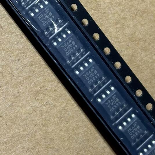
P-ch MOSFET,-30V,-8.1A,24mOhm RDS(on)@-10V,TrenchFET,SOIC-8,无卤素,-55~150C

38787

有效库存
转到查询

Image for reference only

制造商零件:

si4435ddy-t1-ge3

包装:

SOIC-8(SO-8,150 密耳)(4.88 x 3.89 x 1.54 毫米,1.27 毫米间距)

品牌:
产品类别:
您可能感兴趣的其他建议.
说明

Vishay Siliconix 的 SI4435DDY-T1-GE3 是一款 P 沟道 30-V (D-S) TrenchFET 功率 MOSFET,采用 8 引脚 SOIC (SO-8) 封装 (4.88 x 3.89 x 1.54 mm)。根据 IEC 61249-2-21 标准,该器件不含卤素,符合 RoHS 规范。主要规格VDS = -30V,VGS = 正负 20V,ID = -8.1A(PCB 上 TA=25C),-11.4A(散热器上 TC=25C)。RDS(on) = 19.5mOhm 典型值/24mOhm 最大值(VGS=-10V,ID=-9.1A);28mOhm 典型值/35mOhm 最大值(VGS=-4.5V,ID=-6.9A)。栅极阈值电压:-1.0V 至 -3.0V,ID=-250uA。栅极总电荷:VGS=-4.5V 时典型值为 15nC,VGS=-10V 时为 32nC。输入电容:1350pF。正向跨导:23S。本体二极管正向电压:IS=-2A 时典型值为 -0.75V。本体二极管反向恢复:34ns / 22nC 典型值。功率耗散:2.5W(PCB 上 TA=25C),5.0W(TC=25C)。热阻:RthJA = 50C/W max,RthJF = 25C/W max。VGS=-10V 时的开关时间:td(on)=10ns,tr=8ns,td(off)=45ns,典型值 tf=12ns。工作结温:-55℃ 至 +150℃。单脉冲雪崩:20mJ/20A。后缀 -T1-GE3 表示:T1 = 卷带(2500 件),GE3 = 无铅无卤。有源产品,符合 RoHS 和 EAR99 标准。.

The SI4435DDY-T1-GE3 from Vishay Siliconix is a P-channel enhancement-mode TrenchFET power MOSFET rated for -30V drain-source voltage and -8.1A continuous drain current in an SOIC-8 (SO-8) surface-mount package. It is one of the most popular P-channel MOSFETs for load switching and battery management applications, offering an excellent balance of low on-resistance, moderate gate charge, and wide availability.

The TrenchFET technology uses a vertical trench gate structure that significantly reduces the channel resistance compared to planar MOSFET architectures. By etching deep trenches into the silicon and lining them with the gate oxide and gate electrode, the channel is formed on the vertical sidewalls of the trench. This increases the channel width per unit area, reducing the specific on-resistance (RDS(on) x area) and enabling lower RDS(on) in a smaller die. The SI4435DDY achieves 24mOhm maximum RDS(on) at VGS=-10V in a standard SO-8 package, making it suitable for load switching applications where voltage drop and power dissipation must be minimized.

The SO-8 (150mil) package is the industry-standard footprint for medium-power surface-mount MOSFETs. It features a gull-wing lead configuration with three source pins (1-3), one gate pin (4), and four drain pins (5-8) connected to the die attach pad for thermal dissipation. The multiple source and drain pins reduce package parasitic inductance and provide parallel current paths, improving current handling and thermal performance. The LITTLE FOOT designation indicates that this package has been modified to provide the heat transfer capabilities required by power devices.

As a P-channel MOSFET, the SI4435DDY is turned on by applying a negative gate-source voltage (VGS < 0). For a high-side load switch application with a 5V supply, the gate is pulled to GND (VGS = -5V) to turn on the MOSFET, connecting the source (connected to 5V supply) to the drain (connected to the load). When the gate is pulled to the source voltage (VGS = 0V), the MOSFET turns off, disconnecting the load. This simple high-side switching configuration is the primary use case for P-channel MOSFETs, as it avoids the need for a gate drive voltage above the supply rail that N-channel high-side switches require. The RDS(on) specification varies significantly with gate drive voltage. At VGS=-10V, the maximum RDS(on) is 24mOhm, while at VGS=-4.5V, it increases to 35mOhm. For a 5V system where the gate can be driven to GND (VGS=-5V), the RDS(on) falls between these values, typically around 28-30mOhm. This voltage-dependent RDS(on) must be considered in thermal calculations, as higher RDS(on) leads to more power dissipation at the same load current. The gate charge of 15nC at VGS=-4.5V and 32nC at VGS=-10V determines the switching energy and the gate drive current required for a given switching frequency. For load switching applications where the MOSFET switches infrequently (e.g., power-on/off), the gate charge has minimal impact on power dissipation. For PWM applications at higher frequencies, the gate charge must be considered in the total power budget. The body diode (inherent in all MOSFETs) has a forward voltage of 0.75V typical at 2A and a reverse recovery time of 34ns. This body diode can conduct current when VDS is negative (drain below source), which is the normal forward direction for a P-channel MOSFET. In load switching applications, the body diode may briefly conduct during transients before the MOSFET channel fully enhances. The -T1-GE3 suffix provides important ordering information: T1 indicates tape-and-reel packaging (2,500 units per reel), and GE3 indicates both lead-free (per RoHS) and halogen-free (per IEC 61249-2-21). The -E3 suffix (SI4435DDY-T1-E3) is lead-free but not halogen-free. The GE3 variant is preferred for environmentally sensitive applications and regions with strict halogen-free requirements.

The SI4435DDY-T1-GE3 operates as a P-channel enhancement-mode MOSFET using TrenchFET vertical structure technology.

TrenchFET Structure: Unlike planar MOSFETs where the channel is formed on the silicon surface, the TrenchFET uses deep reactive-ion-etched trenches filled with gate polysilicon. The P-body and N+ source regions are formed on the sidewalls of these trenches. When a negative voltage is applied to the gate (relative to the source), an inversion layer (N-type channel) forms along the trench sidewalls, connecting the N+ source to the N- drain epitaxial layer. This vertical current flow path is much shorter than the lateral path in planar devices, reducing the channel resistance. Additionally, the trench structure allows a much higher channel density (channel width per unit die area), which directly reduces the specific on-resistance.

P-Channel Operation: As a P-channel MOSFET, the SI4435DDY has a P+ substrate (drain), P- epitaxial layer (drift region), N-body (channel region), and P+ source diffusion. The gate oxide and gate electrode are formed on the trench sidewalls. When VGS = 0V (gate shorted to source), no inversion layer forms and the device is in the off state. When a negative voltage is applied to the gate (VGS 0 for P-channel, since both VDS and ID are negative in normal operation). The body diode has a forward voltage of 0.75V typical at 2A and can carry continuous current up to 4.1A (TC=25C). The reverse recovery time of 34ns and reverse recovery charge of 22nC are relevant for freewheeling applications where the body diode conducts during each switching cycle.

Avalanche Rating: The device is rated for single-pulse avalanche energy of 20mJ and avalanche current of 20A. Avalanche occurs when the drain-source voltage exceeds the breakdown voltage (-30V), typically during inductive load switching. The avalanche rating indicates the maximum energy the device can absorb in a single event without damage. This is important for unclamped inductive switching applications where voltage spikes may exceed the rated VDS.

针脚 名称 类型 说明
1 S 资料来源 MOSFET source terminal; connect to the higher-potential side of the power rail (e.g., battery positive or VCC rail in high-side switch configuration); internally connected to pins 2 and 3; three source pins reduce package inductance and current density per bond wire; connect all three source pins to the source net on PCB
2 S 资料来源 MOSFET source terminal; internally connected to pins 1 and 3
3 S 资料来源 MOSFET source terminal; internally connected to pins 1 and 2
4 G 大门 MOSFET gate terminal; controls the on/off state of the MOSFET; apply negative voltage relative to source (VGS < -1.0V) to turn on; VGS = 0V to turn off; maximum VGS = plus/minus 20V; gate input capacitance ~1350pF; typical gate resistance 5.8 ohms; drive with low-impedance gate driver for fast switching; add series gate resistor (1-10 ohm) to control dv/dt and reduce EMI
5 D 排水 MOSFET drain terminal; connect to the load side in high-side switch configuration; internally connected to pins 6, 7, and 8 through the die attach pad; four drain pins provide low-inductance current path and thermal connection to PCB; the drain is also the cathode of the body diode
6 D 排水 MOSFET drain terminal; internally connected to pins 5, 7, and 8
7 D 排水 MOSFET drain terminal; internally connected to pins 5, 6, and 8
8 D 排水 MOSFET drain terminal; internally connected to pins 5, 6, and 7
应用 说明
高压侧负载开关 Use as a high-side P-channel load switch to connect/disconnect power rails; source to battery/VCC, drain to load; gate pulled to GND (through resistor or MOSFET driver) to turn on; gate pulled to source to turn off; 24mOhm RDS(on) at VGS=-10V provides very low voltage drop at currents up to 5A; SO-8 package handles 2.5W on PCB; add gate pull-up resistor (10k-100k) to ensure MOSFET stays off during power-up
Battery Disconnect Protect battery from over-discharge or short circuit; source to battery positive, drain to system power rail; gate controlled by battery management IC or voltage supervisor; RDS(on) of 24mOhm results in only 120mV drop at 5A, minimizing power loss in the switch; wide -55C to +150C operating range for automotive and industrial battery systems
H-Bridge Motor Drive (P-Channel Side) Use as high-side P-channel MOSFETs in an H-bridge motor drive circuit; two SI4435DDY devices for the high-side arms, two N-channel MOSFETs for the low-side arms; -30V rating supports 12V/24V motor supplies; 15nC gate charge at VGS=-4.5V enables PWM switching up to 20-50kHz with simple gate drive
Power Path ORing OR multiple power sources by placing a P-channel MOSFET in series with each source; gate controlled by comparator or ideal diode controller that turns off the MOSFET when current attempts to flow in reverse; 24mOhm RDS(on) is much lower than the series resistance of a Schottky diode, reducing voltage drop and power dissipation
Reverse Polarity Protection Use as a reverse polarity protection switch; source to input power, drain to system; gate connected to GND through a Zener diode; when input polarity is correct, MOSFET turns on; when reversed, MOSFET stays off, protecting downstream circuitry; lower voltage drop than series diode protection
模型 制造商 兼容性 主要区别
SI4435DDY-T1-E3 Vishay Same, Not Halogen-Free Identical electrical specifications; lead-free (RoHS) but NOT halogen-free; same SO-8 package; same tape-and-reel; use when halogen-free is not required; may have slightly lower cost
SI4435DY-T1-GE3 Vishay Same in SO-8 (Different Suffix) Same die in possibly different package variant; verify pinout compatibility; different ordering suffix may indicate different testing or packaging
IRF9Z34NPBF 英飞凌 功能相似 P-channel MOSFET; -60V, -18A; 100mOhm RDS(on) at VGS=-10V; higher voltage but higher RDS(on); D2PAK package; use for higher-voltage applications with relaxed RDS(on) requirements
FDS4435 ON 半 插件兼容 P-channel MOSFET; -30V, -8.1A; 22mOhm RDS(on) at VGS=-10V; same SO-8 pinout; very similar specifications; alternative source for second-sourcing
AO4407A Alpha and Omega 插件兼容 P-channel MOSFET; -30V, -12A; 8.5mOhm RDS(on) at VGS=-10V; same SO-8 pinout; lower RDS(on) and higher current; use when lower voltage drop is needed; different gate charge profile
推荐部件
Shielded power inductor, 2.2 uH, 20%, 2525 package, high saturation, low DCR

品牌:

封装:

2525 (6.7 x 7.2 x 3.0 mm)
有库存:
3210pcs

货运周期:3~7 天
最低订购量为 1

转到查询
Dual phototransistor optocoupler, 4kV isolation, 100-200% CTR, 70V BVCEO, SOIC-8

品牌:

封装:

SOIC-8 (5.3 x 6.1 x 1.65mm, 150mil)
有库存:
2409 件

货运周期:3~7 天
最低订购量为 1

转到查询
600W unidirectional TVS, 12V standoff, 19.9V clamp, SMB package

品牌:

封装:

SMB (DO-214AA) (4.6 x 3.9 x 2.3 mm)
有库存:
10042pcs

货运周期:3~7 天
最低订购量为 1

转到查询
5.5×2.5mm DC barrel jack, 15A 24V, right-angle through-hole

品牌:

封装:

Right-Angle Through-Hole (13.7 x 10.5 x 11.0 mm)
有库存:
14723pcs

货运周期:3~7 天
最低订购量为 1

转到查询
3A 40V Schottky diode, 0.5V VF, SMA (DO-214AC) package

品牌:

封装:

SMA (DO-214AC) (5.2 x 2.6 x 2.2 mm)
有库存:
13969pcs

货运周期:3~7 天
最低订购量为 1

转到查询
600W unidirectional TVS, 58V standoff, 93.1V clamp, SMA package

品牌:

封装:

SMA (DO-214AC) (5.2 x 2.6 x 2.2 mm)
有库存:
10975pcs

货运周期:3~7 天
最低订购量为 1

转到查询
质量保证

我们从合作供应链采购的所有电子元件都经过严格的进货检验。通过仔细的测试,我们确保交付给客户的所有产品都是原装正品,符合质量要求。此外,我们还保存完整的检验记录,使整个供应链流程清晰可查。.

认证
我们获得了多项专业认证,并建立了自己的专业检测实验室,确保交付给客户的每一件产品都符合最高质量要求。我们严格按照流程进行检测,确保产品质量稳定、参数准确。为保证原装正品,我们还与可靠的第三方检测机构合作,进行严格的质量检测。我们始终高度重视质量,完全符合行业标准、相关法规和 ISO 9001:2015 的要求。.

发货与付款

我们从合作供应链采购的所有电子元件都经过严格的进货检验。通过仔细的测试,我们确保交付给客户的所有产品都是原装正品,符合质量要求。此外,我们还保存完整的检验记录,使整个供应链流程清晰可查。.

认证
我们获得了多项专业认证,并建立了自己的专业检测实验室,确保交付给客户的每一件产品都符合最高质量要求。我们严格按照流程进行检测,确保产品质量稳定、参数准确。为保证原装正品,我们还与可靠的第三方检测机构合作,进行严格的质量检测。我们始终高度重视质量,完全符合行业标准、相关法规和 ISO 9001:2015 的要求。.

服务与包装

我们从合作供应链采购的所有电子元件都经过严格的进货检验。通过仔细的测试,我们确保交付给客户的所有产品都是原装正品,符合质量要求。此外,我们还保存完整的检验记录,使整个供应链流程清晰可查。.

认证
我们获得了多项专业认证,并建立了自己的专业检测实验室,确保交付给客户的每一件产品都符合最高质量要求。我们严格按照流程进行检测,确保产品质量稳定、参数准确。为保证原装正品,我们还与可靠的第三方检测机构合作,进行严格的质量检测。我们始终高度重视质量,完全符合行业标准、相关法规和 ISO 9001:2015 的要求。.