首页 > 集成电路 IC > CSD87330Q3D

CSD87330Q3D


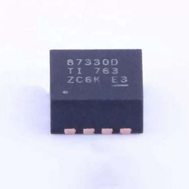
30V 20A NexFET power block, 91% eff@15A, 5V gate drive, LSON-8 3.3x3.3mm, up to 1.5MHz, -55~150°C

4400

有效库存
转到查询

Image for reference only

制造商零件:

CSD87330Q3D

包装:

LSON-CLIP-8(3.3 x 3.3 x 1.0 毫米,焊盘模式见数据表)

品牌:
产品类别:
您可能感兴趣的其他建议.
说明

The CSD87330Q3D from Texas Instruments is a 30-V, 20-A synchronous buck NexFET power block in an 8-pin LSON (3.3×3.3 mm) package. It integrates an asymmetrical dual N-channel MOSFET pair (control FET + sync FET) optimized for 5-V gate drive synchronous buck converters. Key specs include up to 27-V input, 91% system efficiency at 15 A (12-V input, 1.3-V output, 500 kHz), switching frequency up to 1.5 MHz, and 6-W power dissipation. The ultra-low inductance copper-clip package minimizes parasitic ringing. Targeted at POL DC-DC converters, industrial power, and medium-current buck regulators operating from 5-V to 27-V input rails. Operating temperature range is -55°C to +150°C (TJ).

The CSD87330Q3D is a NexFET power block from Texas Instruments that integrates a half-bridge MOSFET pair in a compact 3.3×3.3-mm LSON package. It is the smaller sibling of the CSD87350Q5D (5×6 mm, 40 A), targeting 15-20 A synchronous buck applications where board space is at a premium.

The power block approach integrates both the control FET and sync FET in one package with a copper-clip internal interconnect, reducing parasitic inductance between the two MOSFETs to sub-100 pH. This eliminates the switch-node ringing and overshoot typical of discrete MOSFET solutions, enabling higher switching frequencies and smaller output filter components.

The control FET (Q1) is optimized for low switching losses with gate charge of 4.8 nC typical at 4.5 V, while the sync FET (Q2) is optimized for low conduction losses. The asymmetrical design achieves 91% system efficiency at 15 A output (12 V to 1.3 V at 500 kHz), with only 2 W total power loss under those conditions.

The 3.3×3.3-mm package occupies only 10.89 mm² — less than half the area of the 5×6-mm CSD87350Q5D — making it ideal for point-of-load (POL) converters in space-constrained applications such as notebook VRMs, embedded processor power, and industrial control systems. The exposed thermal pad (PGND) provides 2°C/W junction-to-case thermal resistance for efficient heat removal through the PCB.

The device is rated for 20-A continuous operation and 120-A pulsed current. The 30-V drain-to-source voltage supports 5-V, 12-V, and 19-V input rails. Switching frequency support up to 1.5 MHz enables very small inductors. The device pairs with TI’s TPS53819A and similar controllers for multi-phase VRM, or with any 5-V gate driver for standalone POL converters.

**Half-Bridge Configuration:** The CSD87330Q3D integrates two N-channel MOSFETs in a half-bridge: Q1 (control FET, high-side) connects VIN to SW, Q2 (sync FET, low-side) connects SW to PGND. During Q1 on-time, inductor current flows from VIN through Q1 to the output. During Q2 on-time, inductor current freewheels through Q2.

**Asymmetrical MOSFET Optimization:** Q1 is optimized for fast switching with low gate charge (Qg = 4.8 nC) and moderate RDS(on). Q2 is optimized for low conduction loss with very low RDS(on), since it conducts for a larger fraction of the cycle at low duty cycles. This asymmetry is fundamental to efficient buck converter design.

**Copper Clip Interconnect:** The internal copper clip directly connects the control FET drain to the sync FET drain, reducing loop inductance to sub-100 pH versus 0.5-2 nH for wire-bonded discrete solutions. This dramatically reduces switch-node ringing, allowing faster switching edges without exceeding voltage ratings.

**Gate Drive Interface:** The TG (top gate) and BG (bottom gate) pins connect directly to an external gate driver. The TGR pin is the high-side return (connected to SW). The FETs are optimized for 5-V gate drive with threshold voltages of 1.0 V (Q1) and 0.75 V (Q2). Maximum VGS is 8 V for both FETs.

针脚 名称 类型 说明
1 VSW O Switch node; Q1 source / Q2 drain; connect to output inductor; high dv/dt node; minimize copper area
2 VSW O Switch node (parallel with pin 1); doubled for current capacity
3 VSW O Switch node (parallel with pins 1,2)
4 BG I Bottom gate drive input; drives Q2 (sync FET) gate; connect to gate driver low-side output; referenced to PGND
5 TGR I Top gate return; high-side gate drive return; connects to SW node; bootstrap capacitor return
6 TG I Top gate drive input; drives Q1 (control FET) gate; connect to gate driver high-side output; referenced to TGR
7 PGND G Power ground; Q2 source and thermal pad; connect to PCB ground plane; critical for thermal
8 VIN P Input supply; Q1 drain; connect to input bypass capacitors (ceramic recommended)
垫子 PGND/Thermal G Exposed thermal pad; electrically PGND; solder to PCB ground plane with thermal vias
应用 说明
Notebook POL Converter 5-20A single-phase buck from 12V/19V to 1.0-3.3V for chipset/DIMM rails; pair with LM27403 or TPS53915 driver; 500kHz-1MHz switching; 3.3×3.3mm footprint fits tight laptop PCB
Embedded Processor Core Rail 12V-to-1.2V at 15A for FPGA/SoC core; single-phase with any 5V gate driver; 800kHz reduces inductor size; 91% efficiency limits thermal design burden
Industrial Point-of-Load 24V-to-5V/3.3V buck at 10A for industrial PLC and motor controller logic rails; wide input range to 27V; -55 to 150°C junction range for harsh environments
模型 制造商 兼容性 主要区别
CSD87350Q5D TI 系列升级 40A version in 5x6mm LSON-8; same 30V, 5V gate drive; higher current; larger footprint; use when 20A is insufficient
CSD87334Q3D TI 针脚兼容升级 Same 3.3×3.3mm footprint; optimized for high-duty-cycle apps; similar 20A rating; different RDS(on) balance
CSD87333Q3D TI 针脚兼容替代方案 Same 3.3×3.3mm package; 25A rating; higher current; optimized for high-duty-cycle synchronous buck
FDMF5820A onsemi 功能等效 30V/20A power stage; PQFN 5x5mm; integrated driver+MOSFETs; different pinout; use when integrated driver preferred
推荐部件
PMIC for AM335x, 3 bucks, 2 LDOs, battery charger, WLED, I2C, VQFN-48

品牌:

封装:

VQFN-48 (6×6 mm, 0.4 mm pitch)
有库存:
8909pcs

货运周期:3~7 天
最低订购量为 1

转到查询
Octal D-type flip-flop, edge-triggered, async clear, 28MHz, SOP-20

品牌:

封装:

SOP-20 (NS) (12.6×7.8 mm)
有库存:
8359pcs

货运周期:3~7 天
最低订购量为 1

转到查询
3-to-8 decoder/demux, active-low outputs, 3 enable inputs, 15ns, PDIP-16

品牌:

封装:

PDIP-16 (24.33×9.4 mm, Through-Hole)
有库存:
11952pcs

货运周期:3~7 天
最低订购量为 1

转到查询
2W mono Class-AB audio amp, BTL speaker + SE headphone, 2.5-5.5V, HVSSOP-8

品牌:

封装:

HVSSOP-8 (DGN) (3.0×4.9 mm, PowerPAD)
有库存:
3337pcs

货运周期:3~7 天
最低订购量为 1

转到查询
10/100 Ethernet PHY, MII/RMII/SNI, Auto-MDIX, 270mW, LQFP-48, commercial

品牌:

封装:

LQFP-48 (7×7 mm)
有库存:
14754pcs

货运周期:3~7 天
最低订购量为 1

转到查询
Octal bus transceiver, 3-state outputs, 2-6V, 12ns tpd, TSSOP-20

品牌:

封装:

TSSOP-20 (6.5×6.4 mm)
有库存:
2638pcs

货运周期:3~7 天
最低订购量为 1

转到查询
质量保证

我们从合作供应链采购的所有电子元件都经过严格的进货检验。通过仔细的测试,我们确保交付给客户的所有产品都是原装正品,符合质量要求。此外,我们还保存完整的检验记录,使整个供应链流程清晰可查。.

认证
我们获得了多项专业认证,并建立了自己的专业检测实验室,确保交付给客户的每一件产品都符合最高质量要求。我们严格按照流程进行检测,确保产品质量稳定、参数准确。为保证原装正品,我们还与可靠的第三方检测机构合作,进行严格的质量检测。我们始终高度重视质量,完全符合行业标准、相关法规和 ISO 9001:2015 的要求。.

发货与付款

我们从合作供应链采购的所有电子元件都经过严格的进货检验。通过仔细的测试,我们确保交付给客户的所有产品都是原装正品,符合质量要求。此外,我们还保存完整的检验记录,使整个供应链流程清晰可查。.

认证
我们获得了多项专业认证,并建立了自己的专业检测实验室,确保交付给客户的每一件产品都符合最高质量要求。我们严格按照流程进行检测,确保产品质量稳定、参数准确。为保证原装正品,我们还与可靠的第三方检测机构合作,进行严格的质量检测。我们始终高度重视质量,完全符合行业标准、相关法规和 ISO 9001:2015 的要求。.

服务与包装

我们从合作供应链采购的所有电子元件都经过严格的进货检验。通过仔细的测试,我们确保交付给客户的所有产品都是原装正品,符合质量要求。此外,我们还保存完整的检验记录,使整个供应链流程清晰可查。.

认证
我们获得了多项专业认证,并建立了自己的专业检测实验室,确保交付给客户的每一件产品都符合最高质量要求。我们严格按照流程进行检测,确保产品质量稳定、参数准确。为保证原装正品,我们还与可靠的第三方检测机构合作,进行严格的质量检测。我们始终高度重视质量,完全符合行业标准、相关法规和 ISO 9001:2015 的要求。.









