首页 > 集成电路 IC > TXS0102DCUR

TXS0102DCUR


2 位双向电平转换器,1.65-3.6V A / 2.3-5.5V B,24Mbps 推挽式,自动定向,VSSOP-8,-40~85°C

8000

有效库存
转到查询

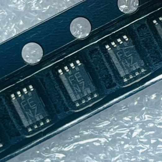
Image for reference only

制造商零件:

TXS0102DCUR

包装:

VSSOP-8(DCU)(2.3 x 2.0 x 0.9 毫米,0.5 毫米间距)

品牌:
您可能感兴趣的其他建议.
说明

The TXS0102DCUR from Texas Instruments is a 2-bit bidirectional voltage-level translator for open-drain and push-pull applications in an 8-pin VSSOP (DCU) package. It supports A-port voltages from 1.65 V to 3.6 V (VCCA) and B-port voltages from 2.3 V to 5.5 V (VCCB), enabling translation between 1.8-V, 2.5-V, 3.3-V, and 5-V logic nodes without direction control. Maximum data rates are 24 Mbps (push-pull) and 2 Mbps (open-drain). Features include VCC isolation, partial-power-down Ioff support, no power-supply sequencing requirement, and ESD protection up to 8-kV HBM on the B port. Operating temperature range is -40°C to +85°C.

The TXS0102DCUR is a 2-bit bidirectional voltage-level translator from Texas Instruments designed for mixed-voltage systems where I²C, UART, GPIO, or other digital signals must cross between different voltage domains. It requires no direction-control signal — each channel automatically senses and translates in both directions, simplifying board design.

The A port operates from 1.65 V to 3.6 V (tracking VCCA), and the B port operates from 2.3 V to 5.5 V (tracking VCCB), with the constraint VCCA ≤ VCCB. This covers all common logic voltage combinations: 1.8 V-to-3.3 V, 1.8 V-to-5 V, 3.3 V-to-5 V, and 2.5 V-to-3.3 V.

The TXS architecture uses passive pass-transistor switches with edge-rate accelerators. For open-drain buses (I²C, SMBus), the pass-FET provides a low-impedance path and the one-shot accelerator briefly turns on a strong pull-up to speed rising edges, achieving up to 2 Mbps. For push-pull signals (UART, SPI, GPIO), the accelerator provides fast edges up to 24 Mbps.

The VCC isolation feature ensures that if either VCCA or VCCB is at GND, both ports enter a high-impedance state, preventing back-feeding. The Ioff circuitry supports partial-power-down mode, allowing one side to be powered down while the other remains active without leakage. No power-supply sequencing is required — either rail can ramp first.

ESD protection is asymmetric: the A port provides 2.5-kV HBM, while the B port (facing the higher-voltage, often external-facing side) provides 8-kV HBM. The OE pin, when pulled low, places all I/Os in high-impedance state with reduced quiescent current. The VSSOP-8 (DCU) package occupies only 4.6 mm² of board area, making it ideal for space-constrained portable designs.

**Pass-FET Switch Core:** Each channel consists of an N-channel pass transistor connecting the A and B sides. The pass-FET gate is biased at a voltage between VCCA and VCCB, allowing bidirectional current flow when either side drives low. The on-resistance is approximately 10 Ω, providing a low-impedance path for DC and low-frequency signals.

**Edge-Rate Accelerator:** One-shot circuits on each side detect falling edges and briefly turn on a strong pull-down (≈ 30 mA for ~30 ns) to accelerate the transition. For rising edges on open-drain buses, the accelerator briefly turns on a strong pull-up to overcome the weak external pull-up resistor. This enables 2 Mbps on I²C at 3.3-V/5-V translation.

**Auto-Direction Detection:** The TXS translator has no explicit direction control. The pass-FET inherently allows either side to drive the bus low. When neither side is driving, the external pull-up resistors (for open-drain) or the driving device (for push-pull) pull the line high through the pass-FET. This transparent operation eliminates the need for a DIR pin.

**VCC Isolation and Ioff:** When either supply is at GND, an internal circuit detects the condition and opens the pass-FET, placing both I/Os in high-impedance. The Ioff feature ensures that no leakage current flows from the powered side to the unpowered side, which is critical for hot-swap and battery-backup applications.

针脚 名称 类型 说明
1 VCCA P A-port supply (1.65-3.6V); powers A-side I/O buffers and OE input logic; bypass with 0.1µF ceramic to GND
2 A1 输入/输出 Channel 1 A-port I/O; voltage referenced to VCCA; connects to low-voltage side of signal
3 A2 输入/输出 Channel 2 A-port I/O; voltage referenced to VCCA
4 接地 G 接地;连接至 PCB 地平面
5 B2 输入/输出 Channel 2 B-port I/O; voltage referenced to VCCB; connects to high-voltage side of signal
6 B1 输入/输出 Channel 1 B-port I/O; voltage referenced to VCCB
7 VCCB P B-port supply (2.3-5.5V); powers B-side I/O buffers; must be ≥ VCCA; bypass with 0.1µF ceramic to GND
8 OE I Output enable (active high); referenced to VCCA; tie to GND via pull-down resistor for safe power-up; internal pull-up to VCCA; pull low to disable all I/Os (Hi-Z)
应用 说明
I²C/SMBus Level Shifting Bridge 1.8V or 3.3V MCU I²C bus to 5V peripheral; auto-direction handles bidirectional SDA without DIR pin; 2Mbps supports 1MHz Fast-mode Plus; pull-up resistors on both sides set idle-high levels
UART Cross-Voltage Communication Translate 3.3V MCU UART TX/RX to 5V GPS module or cellular modem; push-pull mode supports 24Mbps; OE pin allows MCU to tri-state bus for shared UART lines
GPIO Voltage Adapter Interface 1.8V SoC GPIOs to 3.3V or 5V sensors and displays; both channels independently handle mixed open-drain and push-pull signals; VCC isolation protects SoC when peripheral power is off
模型 制造商 兼容性 主要区别
TXS0102DCTT TI 引脚兼容,相同模具 SSOP-8 package (2.95×2.80mm vs VSSOP 2.3×2.0mm); same electrical specs; use when SSOP footprint preferred
TXS0108EPW TI Functional Upgrade, 8-bit 8-channel version; TSSOP-20; same VCCA/VCCB ranges; auto-direction; use when more channels needed in single package
PCA9306DCUR TI 功能等效 2-bit bidirectional; VSSOP-8; open-drain only (no push-pull); requires external pull-ups; use for I²C-only applications
SN74LVC1T45DBVR TI 竞争性替代方案 1-bit with DIR pin (direction control); SOT-23-6; 200Mbps; requires direction signal; use for high-speed unidirectional translation
推荐部件
3-16S battery monitor/protector, Li-Ion/LiFePO4, 2 ADCs, TQFP-48

品牌:

封装:

TQFP-48 (7 x 7 x 1.0 mm)
有库存:
2150pcs

货运周期:3~7 天
最低订购量为 1

转到查询
I2C 4.5A 1-cell Li-ion charger, NVDC power path, USB OTG, VQFN-24

品牌:

封装:

VQFN-24 (4.0 x 4.0 x 0.75 mm, with thermal pad)
有库存:
4182pcs

货运周期:3~7 天
最低订购量为 1

转到查询
Single micropower RRIO op-amp, 2.7-10V, 65kHz, 11uA, SOT-23-5

品牌:

封装:

SOT-23-5 (2.9 x 2.8 x 1.15 mm)
有库存:
8750pcs

货运周期:3~7 天
最低订购量为 1

转到查询
Single 2-input AND gate, 1.65-5.5V, 24mA drive, SOT-23-5, LVC

品牌:

封装:

SOT-23-5 (2.9 x 1.6 x 1.15 mm)
有库存:
35000 件

货运周期:3~7 天
最低订购量为 1

转到查询
8-bit parallel-load shift register, PISO, 2-6V, 24 MHz, SOIC-16

品牌:

封装:

SOIC-16 (9.9 x 6.0 mm)
有库存:
4837pcs

货运周期:3~7 天
最低订购量为 1

转到查询
Quad differential line receiver, EIA-422/423, 3-state TTL outputs, 5V, SOIC-16

品牌:

封装:

SOIC-16 (9.9 x 6.0 mm)
有库存:
0 件

货运周期:3~7 天
最低订购量为 1

转到查询
质量保证

我们从合作供应链采购的所有电子元件都经过严格的进货检验。通过仔细的测试,我们确保交付给客户的所有产品都是原装正品,符合质量要求。此外,我们还保存完整的检验记录,使整个供应链流程清晰可查。.

认证
我们获得了多项专业认证,并建立了自己的专业检测实验室,确保交付给客户的每一件产品都符合最高质量要求。我们严格按照流程进行检测,确保产品质量稳定、参数准确。为保证原装正品,我们还与可靠的第三方检测机构合作,进行严格的质量检测。我们始终高度重视质量,完全符合行业标准、相关法规和 ISO 9001:2015 的要求。.

发货与付款

我们从合作供应链采购的所有电子元件都经过严格的进货检验。通过仔细的测试,我们确保交付给客户的所有产品都是原装正品,符合质量要求。此外,我们还保存完整的检验记录,使整个供应链流程清晰可查。.

认证
我们获得了多项专业认证,并建立了自己的专业检测实验室,确保交付给客户的每一件产品都符合最高质量要求。我们严格按照流程进行检测,确保产品质量稳定、参数准确。为保证原装正品,我们还与可靠的第三方检测机构合作,进行严格的质量检测。我们始终高度重视质量,完全符合行业标准、相关法规和 ISO 9001:2015 的要求。.

服务与包装

我们从合作供应链采购的所有电子元件都经过严格的进货检验。通过仔细的测试,我们确保交付给客户的所有产品都是原装正品,符合质量要求。此外,我们还保存完整的检验记录,使整个供应链流程清晰可查。.

认证
我们获得了多项专业认证,并建立了自己的专业检测实验室,确保交付给客户的每一件产品都符合最高质量要求。我们严格按照流程进行检测,确保产品质量稳定、参数准确。为保证原装正品,我们还与可靠的第三方检测机构合作,进行严格的质量检测。我们始终高度重视质量,完全符合行业标准、相关法规和 ISO 9001:2015 的要求。.



