首页 > 集成电路 IC > ATMEGA88PA-PU

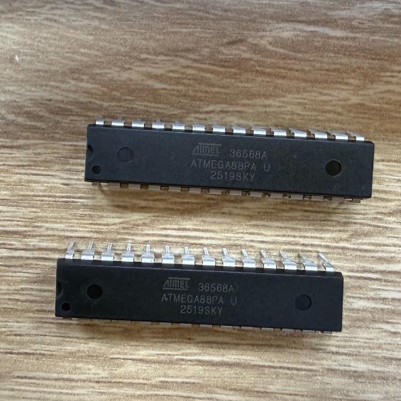
ATMEGA88PA-PU


8 位 AVR picoPower MCU,8KB 闪存,512B EEPROM,1KB SRAM,20MHz,1.8-5.5V,6 通道 10 位 ADC,USART/SPI/I2C,6 PWM,28-PDIP,-40~85C

3827

有效库存
转到查询

Image for reference only

制造商零件:

ATMEGA88PA-PU

包装:

PDIP-28(37.4 x 6.76 x 3.28 毫米,2.54 毫米间距)

品牌:
产品类别:
您可能感兴趣的其他建议.
说明

The ATMEGA88PA-PU from Microchip Technology (formerly Atmel) is a high-performance, low-power 8-bit AVR RISC microcontroller with picoPower technology in a 28-pin PDIP through-hole package (37.4 x 6.76 x 3.28 mm). Key specifications: 8 KB ISP Flash memory with read-while-write capability; 512 bytes EEPROM; 1 KB SRAM; 23 programmable I/O lines; 32 general-purpose working registers; operating voltage 1.8V to 5.5V; maximum clock frequency 20 MHz (up to 20 MIPS throughput). Three flexible timer/counters: two 8-bit (Timer0, Timer2) with compare mode, and one 16-bit (Timer1) with compare and capture mode. Six PWM channels. 10-bit ADC with 6 channels (PDIP package) or 8 channels (TQFP/QFN). Programmable serial USART. Master/Slave SPI serial interface (2 SPI). Byte-oriented 2-wire serial interface (I2C compatible). Programmable watchdog timer with separate on-chip oscillator. On-chip analog comparator. Five software selectable power saving modes: Idle, ADC Noise Reduction, Power-save, Power-down, and Standby. Low power consumption at 1 MHz, 1.8V, 25C: Active 0.2 mA, Power-down 0.1 uA, Power-save 0.75 uA (including 32 kHz RTC). Flash endurance 10,000 write/erase cycles; EEPROM endurance 100,000 cycles; data retention 20 years at 85C. Operating temperature -40C to +85C. ECOPACK2 / RoHS compliant. EAR99. Active product in production.

The ATMEGA88PA-PU from Microchip Technology is a high-performance, low-power 8-bit AVR RISC microcontroller that belongs to the picoPower family, designed for applications where power consumption is a critical design parameter. It is the 28-pin PDIP through-hole version of the ATmega88PA, offering 8 KB of ISP Flash, 512 bytes of EEPROM, and 1 KB of SRAM.

The ATMEGA88PA is part of the widely-used ATmega48/88/168/328 family, which shares the same AVR core and peripheral set with different memory densities. The ATmega88PA sits between the ATmega48PA (4KB Flash) and the ATmega168PA (16KB Flash) / ATmega328P (32KB Flash), providing a cost-effective option for applications that need more than 4KB of program memory but do not require the full 32KB of the ATmega328P.

The AVR RISC architecture achieves near 1 MIPS per MHz throughput by executing most instructions in a single clock cycle. The 32 general-purpose working registers are directly connected to the ALU, allowing two independent registers to be accessed in one instruction executed in one clock cycle. This architecture is significantly more code-efficient than conventional CISC microcontrollers, achieving throughputs up to ten times faster at the same clock frequency.

The picoPower technology is a key differentiator of this device family. It enables ultra-low power consumption through multiple mechanisms: (1) a very low-power oscillator that can run at 32 kHz; (2) sleep modes with current consumption as low as 0.1 uA in Power-down mode; (3) the ability to keep the RTC running in Power-save mode at only 0.75 uA; (4) fast wake-up from sleep modes (6 clock cycles from Idle). These features make the ATMEGA88PA-PU ideal for battery-powered applications where the MCU spends most of its time in a low-power state.

The 28-pin PDIP package is particularly popular among hobbyists, educators, and prototyping environments because it can be easily inserted into breadboards and sockets for quick development and testing. The through-hole package also simplifies hand soldering and rework, making it suitable for low-volume production where automated SMT assembly is not cost-effective. However, the PDIP package only exposes 6 ADC channels (vs 8 in TQFP/QFN) because ADC6 and ADC7 are only available on the 32-pin packages.

The ATMEGA88PA is upward-compatible with the ATmega328P (the MCU used on the Arduino Uno). Code written for the ATmega88PA can generally run on the ATmega328P with minimal changes, and vice versa, as long as the memory constraints of the 88PA (8KB Flash, 1KB SRAM) are respected. This compatibility allows developers to prototype on Arduino platforms and then cost-reduce the design by migrating to the ATmega88PA for production.

The in-system programmable (ISP) Flash allows the device to be programmed without removing it from the circuit, using only the SPI interface (MOSI, MISO, SCK, RESET). This simplifies manufacturing and field updates. The boot loader section supports self-programming, enabling firmware updates over UART, USB, or any other communication interface without external programming hardware.

The ATMEGA88PA-PU operates as an 8-bit Harvard-architecture RISC microcontroller with separate program and data memory spaces.

AVR RISC Core: The AVR core uses a 2-stage pipeline (fetch and execute) and a reduced instruction set where most instructions execute in a single clock cycle. The core features 32 x 8-bit general-purpose working registers (R0-R31) that are directly connected to the ALU. Six of these registers (R26-R31) can also serve as three 16-bit indirect address register pointers (X, Y, Z) for data space addressing. The single-cycle instruction execution means that the effective throughput approaches 1 MIPS per MHz, so at 20 MHz the device delivers approximately 20 MIPS.

Harvard Architecture: The program memory (8KB Flash) and data memory (1KB SRAM + 512B EEPROM + I/O registers) are in separate address spaces. The Flash is organized as 4K x 16-bit words (since AVR instructions are 16 bits wide). The data memory space is a linear address space that includes 32 general-purpose registers, 64 I/O registers, 160 extended I/O registers, and 1KB of SRAM. The EEPROM is accessed through special I/O registers (EEAR, EEDR, EECR) and has its own address space (0-511).

picoPower Technology: The picoPower feature set reduces power consumption through several mechanisms: (1) a precision internal oscillator that can run at 32 kHz with only 0.75 uA current; (2) clock gating that shuts down clocks to unused peripherals; (3) an event system that allows peripherals to interact without CPU intervention; (4) sleep modes with progressively lower power consumption. The Power-down mode stops all clocks and oscillators, achieving 0.1 uA. The Power-save mode keeps the 32 kHz oscillator running for the RTC while stopping all other clocks, achieving 0.75 uA. The ADC Noise Reduction mode stops the CPU but keeps the ADC and its clock running for low-noise conversions.

I/O Port Architecture: Each I/O port (PORTB, PORTC, PORTD) has three associated registers: DDRx (Data Direction), PORTx (Data), and PINx (Port Input). When a pin is configured as output (DDRx bit = 1), the PORTx register drives the pin high or low. When configured as input (DDRx bit = 0), the PORTx bit controls the internal pull-up resistor (1 = pull-up enabled). The PINx register reads the actual pin level regardless of direction. Most I/O pins have alternate functions (USART, SPI, I2C, ADC, timers, interrupts) that can be selected by enabling the corresponding peripheral.

Timer/Counter Architecture: The three timer/counters provide timing and PWM capabilities. Timer0 and Timer2 are 8-bit with prescaler, compare match, and waveform generation modes. Timer1 is 16-bit with additional input capture and PWM modes. All timers support PWM output generation using compare match and waveform generation modes. Timer1 supports 16-bit PWM with input capture for frequency and period measurement. Timer2 can use an external 32 kHz crystal as its clock source for real-time counting applications.

ADC Architecture: The 10-bit successive approximation ADC converts analog inputs in 13-260 us depending on the prescaler setting. The ADC features a multiplexer that selects one of 6 (PDIP) or 8 (TQFP/QFN) input channels. A temperature sensor is also available as an ADC input channel. The ADC can operate in single-conversion or free-running mode, and can be triggered by an external signal or a timer compare match. In ADC Noise Reduction sleep mode, the CPU is halted during conversion to minimize digital noise.

In-System Programming (ISP): The Flash and EEPROM can be programmed via the SPI interface while the device is mounted in the target system. During ISP programming, the RESET pin must be held low, and serial data is clocked into the device via MOSI while SCK provides the clock. The ISP protocol allows read, write, erase, and verify operations on both Flash and EEPROM. A fuse system controls device configuration including clock source, startup time, brown-out detection level, and memory partitioning.

针脚 名称 类型 说明
1 PC6 (RESET/PCINT14) I/O (Reset) Port C bit 6; default function is active-low RESET input (when RSTDISBL fuse is unprogrammed); a low level longer than the minimum pulse length generates a reset; if RSTDISBL fuse is programmed, this pin becomes a general-purpose I/O with different electrical characteristics than other Port C pins; connect 10k pull-up to VCC and optional reset button to GND
2 PD0 (RXD/PCINT16) 输入/输出 Port D bit 0; alternate: USART receive data input (RXD); Pin Change Interrupt 16; when USART is enabled, this pin receives serial data; in general I/O mode, standard bidirectional pin with optional pull-up
3 PD1 (TXD/PCINT17) 输入/输出 Port D bit 1; alternate: USART transmit data output (TXD); Pin Change Interrupt 17; when USART is enabled, this pin transmits serial data; in general I/O mode, standard bidirectional pin
4 PD2 (INT0/PCINT18) 输入/输出 Port D bit 2; alternate: External Interrupt 0 input (INT0), supports rising/falling/low-level trigger; Pin Change Interrupt 18; commonly used for wake-up from sleep on external event
5 PD3 (OC2B/INT1/PCINT19) 输入/输出 Port D bit 3; alternate: Timer/Counter2 Output Compare B (OC2B) for PWM output; External Interrupt 1 (INT1); Pin Change Interrupt 19
6 PD4 (XCK/T0/PCINT20) 输入/输出 Port D bit 4; alternate: USART external clock (XCK) in synchronous mode; Timer/Counter0 external clock input (T0); Pin Change Interrupt 20
7 VCC 电源 Digital supply voltage; connect to 1.8V-5.5V supply; bypass with 100nF ceramic capacitor to GND close to pin
8 接地 地面 接地;连接至 PCB 地平面
9 PB6 (XTAL1/TOSC1/PCINT6) 输入/输出 Port B bit 6; alternate: external high-frequency crystal oscillator input (XTAL1) or low-frequency timer oscillator input (TOSC1); Pin Change Interrupt 6; when using external crystal, connect to crystal and load capacitors
10 PB7 (XTAL2/TOSC2/PCINT7) 输入/输出 Port B bit 7; alternate: external high-frequency crystal oscillator output (XTAL2) or low-frequency timer oscillator output (TOSC2); Pin Change Interrupt 7; when using external crystal, connect to crystal and load capacitors
11 PD5 (OC0B/T1/PCINT21) 输入/输出 Port D bit 5; alternate: Timer/Counter0 Output Compare B (OC0B) for PWM; Timer/Counter1 external clock input (T1); Pin Change Interrupt 21
12 PD6 (OC0A/AIN0/PCINT22) 输入/输出 Port D bit 6; alternate: Timer/Counter0 Output Compare A (OC0A) for PWM; Analog Comparator positive input (AIN0); Pin Change Interrupt 22
13 PD7 (AIN1/PCINT23) 输入/输出 Port D bit 7; alternate: Analog Comparator negative input (AIN1); Pin Change Interrupt 23; used with AIN0 for analog comparison without ADC
14 PB0 (CLKO/ICP1/PCINT0) 输入/输出 Port B bit 0; alternate: System clock output (CLKO) when CKOUT fuse is programmed; Timer/Counter1 Input Capture (ICP1); Pin Change Interrupt 0
15 PB1 (OC1A/PCINT1) 输入/输出 Port B bit 1; alternate: Timer/Counter1 Output Compare A (OC1A) for 16-bit PWM; Pin Change Interrupt 1
16 PB2 (SS/OC1B/PCINT2) 输入/输出 Port B bit 2; alternate: SPI Slave Select input (SS); Timer/Counter1 Output Compare B (OC1B) for PWM; Pin Change Interrupt 2
17 PB3 (MOSI/OC2A/PCINT3) 输入/输出 Port B bit 3; alternate: SPI Master Out Slave In (MOSI); Timer/Counter2 Output Compare A (OC2A) for PWM; Pin Change Interrupt 3; also used for ISP programming data input
18 PB4 (MISO/PCINT4) 输入/输出 Port B bit 4; alternate: SPI Master In Slave Out (MISO); Pin Change Interrupt 4; also used for ISP programming data output
19 PB5 (SCK/PCINT5) 输入/输出 Port B bit 5; alternate: SPI Serial Clock (SCK); Pin Change Interrupt 5; also used for ISP programming clock
20 AVCC 电源 Analog supply voltage for ADC and Port A (if present); should be connected to VCC even if ADC is not used; if ADC is used, connect through an LC filter to VCC for reduced noise; must not differ from VCC by more than 0.3V
21 AREF Analog Ref Analog reference input for ADC; can be connected to external reference voltage (0-VCC) or left unconnected (internal VCC reference used); decouple with 100nF capacitor to GND; do not connect to a voltage lower than GND
22 接地 地面 Ground (analog ground); connect to PCB ground plane
23 PC0 (ADC0/PCINT8) 输入/输出 Port C bit 0; alternate: ADC input channel 0; Pin Change Interrupt 8; 10-bit ADC with conversion range 0-VCC
24 PC1 (ADC1/PCINT9) 输入/输出 Port C bit 1; alternate: ADC input channel 1; Pin Change Interrupt 9
25 PC2 (ADC2/PCINT10) 输入/输出 Port C bit 2; alternate: ADC input channel 2; Pin Change Interrupt 10
26 PC3 (ADC3/PCINT11) 输入/输出 Port C bit 3; alternate: ADC input channel 3; Pin Change Interrupt 11
27 PC4 (ADC4/SDA/PCINT12) 输入/输出 Port C bit 4; alternate: ADC input channel 4; Two-Wire Interface (I2C) data line (SDA); Pin Change Interrupt 12; open-drain output when I2C is enabled; requires external pull-up resistor
28 PC5 (ADC5/SCL/PCINT13) 输入/输出 Port C bit 5; alternate: ADC input channel 5; Two-Wire Interface (I2C) clock line (SCL); Pin Change Interrupt 13; open-drain output when I2C is enabled; requires external pull-up resistor
应用 说明
Arduino-Compatible Custom Board Design a cost-reduced Arduino-compatible board using ATMEGA88PA-PU instead of ATmega328P; 8KB Flash sufficient for many Arduino sketches; compatible with Arduino IDE via MiniCore board package; 28-PDIP fits standard Arduino socket; save component cost by using only the memory density actually needed; suitable for products that need Arduino compatibility but not 32KB Flash
Battery-Powered Sensor Node Leverage picoPower technology for ultra-long battery life; MCU sleeps in Power-down mode (0.1 uA) between sensor readings; wakes on pin-change interrupt from sensor or RTC; takes ADC reading, transmits via USART or I2C, returns to sleep; 1KB SRAM sufficient for sensor data buffering; operates down to 1.8V allowing direct single-cell Li-ion or 2xAAA operation
Industrial Control Interface Use multiple I/O pins for relay control, LED indicators, and switch inputs; USART for Modbus RTU communication; I2C for connecting external I/O expanders; SPI for connecting external ADC or DAC; internal ADC for analog sensor monitoring; watchdog timer for safety-critical operation; brown-out detection prevents erratic behavior during power supply dips
Consumer Electronics Remote Control Implement IR or RF remote control with keypad scanning and LED feedback; 23 I/O pins for matrix keypad and indicator LEDs; Timer1 generates 38kHz IR carrier frequency via PWM; USART for RF module communication; Power-down mode between key presses maximizes battery life; internal oscillator eliminates need for external crystal
Smart Home Sensor Temperature, humidity, and light sensing with periodic wireless transmission; ADC reads analog sensors; I2C connects digital sensors (e.g., BME280); USART communicates with wireless module (e.g., HC-12, nRF24L01); Power-save mode with 32kHz RTC for timed wake-up; 512-byte EEPROM stores calibration data and configuration
模型 制造商 兼容性 主要区别
ATMEGA48PA-PU 微型芯片 Pin-Compatible, Less Memory Same 28-PDIP pinout and peripherals; only 4KB Flash and 256B EEPROM (vs 8KB/512B); same 1KB SRAM; use when 4KB Flash is sufficient; lower cost; fully software-compatible with reduced memory
ATMEGA168PA-PU 微型芯片 Pin-Compatible, More Flash Same 28-PDIP pinout and peripherals; 16KB Flash and 512B EEPROM; 1KB SRAM; double the Flash of ATmega88PA; use when 8KB is insufficient; same peripheral set; drop-in replacement
ATMEGA328P-PU 微型芯片 Pin-Compatible, Maximum Memory Same 28-PDIP pinout; 32KB Flash, 1KB EEPROM, 2KB SRAM; the Arduino Uno MCU; maximum memory in the family; use when largest code space and SRAM are needed; most popular and widely stocked variant
ATMEGA88PA-AU 微型芯片 Same Die, TQFP Package Same ATmega88PA die in 32-pin TQFP (7x7mm) surface-mount package; exposes 2 additional ADC channels (ADC6, ADC7) for 8 total; SMD package for automated assembly; same electrical specifications; use for production designs
ATtiny84A-PU 微型芯片 Smaller AVR Alternative 14-pin DIP, 8KB Flash, 512B EEPROM, 512B SRAM; fewer I/O pins (12 vs 23); 8-channel 10-bit ADC; no USART; USI instead of full I2C/SPI; lower cost; use when fewer pins and no USART are needed
推荐部件
Dual 12-bit DAC, SPI, 2.7-5.5V, 4.5us settling, SOIC-14, AEC-Q100

品牌:

封装:

SOIC-14 (8.65 x 3.9 x 1.5 mm)
有库存:
6368pcs

货运周期:3~7 天
最低订购量为 1

转到查询
14-pin 8-bit PIC MCU, 1792B Flash, 128B SRAM, 10-bit ADC, PDIP-14, industrial

品牌:

封装:

PDIP-14 (19.18 x 6.35 mm)
有库存:
5620pcs

货运周期:3~7 天
最低订购量为 1

转到查询
4Mbit (512Kx8) Multi-Purpose Flash, 2.7-3.6V, 70ns, PLCC-32, SuperFlash

品牌:

封装:

PLCC-32 (11.43 x 13.21 mm)
有库存:
330pcs

货运周期:3~7 天
最低订购量为 1

转到查询
8-bit AVR MCU, 20 MHz, 32KB Flash, 2KB SRAM, TQFP-32, 1.8-5.5V

品牌:

封装:

TQFP-32 (7 x 7 x 1.0 mm)
有库存:
13892pcs

货运周期:3~7 天
最低订购量为 1

转到查询
E1/T1 Line Interface Unit, 8.192Mbps, short/long haul, integrated CDR, 80-MQFP, 3.3V

品牌:

封装:

80-MQFP (14x14mm)
有库存:
14099pcs

货运周期:3~7 天
最低订购量为 1

转到查询
ARM7TDMI MCU, 55MHz, 256KB Flash, 64KB SRAM, Ethernet MAC, USB, CAN, LQFP-100

品牌:

封装:

LQFP-100
有库存:
3752pcs

货运周期:3~7 天
最低订购量为 1

转到查询
质量保证

我们从合作供应链采购的所有电子元件都经过严格的进货检验。通过仔细的测试,我们确保交付给客户的所有产品都是原装正品,符合质量要求。此外,我们还保存完整的检验记录,使整个供应链流程清晰可查。.

认证
我们获得了多项专业认证,并建立了自己的专业检测实验室,确保交付给客户的每一件产品都符合最高质量要求。我们严格按照流程进行检测,确保产品质量稳定、参数准确。为保证原装正品,我们还与可靠的第三方检测机构合作,进行严格的质量检测。我们始终高度重视质量,完全符合行业标准、相关法规和 ISO 9001:2015 的要求。.

发货与付款

我们从合作供应链采购的所有电子元件都经过严格的进货检验。通过仔细的测试,我们确保交付给客户的所有产品都是原装正品,符合质量要求。此外,我们还保存完整的检验记录,使整个供应链流程清晰可查。.

认证
我们获得了多项专业认证,并建立了自己的专业检测实验室,确保交付给客户的每一件产品都符合最高质量要求。我们严格按照流程进行检测,确保产品质量稳定、参数准确。为保证原装正品,我们还与可靠的第三方检测机构合作,进行严格的质量检测。我们始终高度重视质量,完全符合行业标准、相关法规和 ISO 9001:2015 的要求。.

服务与包装

我们从合作供应链采购的所有电子元件都经过严格的进货检验。通过仔细的测试,我们确保交付给客户的所有产品都是原装正品,符合质量要求。此外,我们还保存完整的检验记录,使整个供应链流程清晰可查。.

认证
我们获得了多项专业认证,并建立了自己的专业检测实验室,确保交付给客户的每一件产品都符合最高质量要求。我们严格按照流程进行检测,确保产品质量稳定、参数准确。为保证原装正品,我们还与可靠的第三方检测机构合作,进行严格的质量检测。我们始终高度重视质量,完全符合行业标准、相关法规和 ISO 9001:2015 的要求。.









