首页 > 集成电路 IC > AT89C2051-24PU

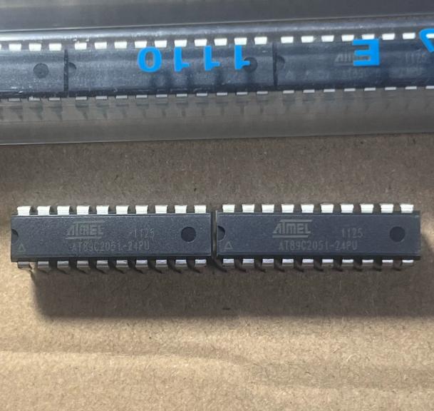
AT89C2051-24PU


8051 8 位 MCU、2KB 闪存、128B RAM、15 个 I/O、2x 16 位定时器、UART、模拟比较器、24MHz、20-PDIP、-40~85C

12650

有效库存
转到查询

Image for reference only

制造商零件:

AT89C2051-24PU

包装:

20 引脚 PDIP(0.300 英寸,7.62 毫米)(26.92 x 7.11 x 4.95 毫米)

品牌:
您可能感兴趣的其他建议.
说明

The AT89C2051-24PU from Microchip Technology (formerly Atmel) is a low-voltage, high-performance CMOS 8-bit microcontroller based on the industry-standard MCS-51 (8051) instruction set, in a 20-pin PDIP package. It features 2KB of in-system programmable Flash memory, 128 bytes of RAM, 15 programmable I/O lines, two 16-bit timer/counters, a full-duplex UART serial port, 6 interrupt sources, and an on-chip analog comparator. Fully static operation from 0Hz to 24MHz. Operating voltage: 4V to 6V (2.7V to 6V for some variants). Two software-selectable power-saving modes: Idle mode (CPU halted, peripherals active) and Power-down mode (oscillator stopped, RAM preserved, wakes on hardware reset). The -24PU suffix indicates 24MHz maximum frequency, PDIP package, industrial temperature range (-40C to 85C). Two-level program memory lock for code protection. Direct LED drive capability (20mA sink per I/O pin). Active product. Pb-free, RoHS compliant.

The AT89C2051-24PU from Microchip Technology (formerly Atmel) is a low-voltage, high-performance CMOS 8-bit microcontroller that implements the industry-standard MCS-51 (8051) instruction set in a compact 20-pin DIP package. The device is manufactured using Microchip’s high-density nonvolatile memory technology and is compatible with the industry-standard 80C51 instruction set and pinout (where applicable given the reduced pin count).

The AT89C2051 is essentially a stripped-down version of the AT89C51, reducing the 40-pin DIP to a 20-pin DIP by eliminating Port 0 and Port 2 (which are primarily used for external memory access in the full 8051). This makes the AT89C2051 ideal for applications that do not require external program or data memory and need a smaller footprint.

Key features include 2KB of on-chip Flash program memory (endurance: 1,000 write/erase cycles), 128 bytes of on-chip RAM, 15 programmable I/O lines (8 from Port 1 and 7 from Port 3; P3.6 is internally connected to the comparator output and not accessible as a general I/O), two 16-bit timer/counters (Timer 0 and Timer 1), a full-duplex UART serial port, and 6 interrupt sources (External Interrupt 0, External Interrupt 1, Timer 0 Overflow, Timer 1 Overflow, Serial Port, and Comparator).

A distinctive feature is the on-chip precision analog comparator, which compares the voltages on P1.0 (AIN0, positive input) and P1.1 (AIN1, negative input). The comparator output is internally connected to P3.6 and can trigger an interrupt. This allows simple analog functions such as zero-crossing detection, battery low-voltage detection, or sensor threshold monitoring without an external comparator IC.

The I/O ports can each sink 20mA, providing direct LED drive capability without external transistor buffers. This is particularly useful for simple indicator and display applications. Port 1 pins P1.2 through P1.7 have internal pull-up resistors and can be used as inputs when logic 1 is written to the port latch. Pins P1.0 and P1.1 do not have internal pull-ups (they serve as comparator inputs) and require external pull-up resistors when used as digital inputs.

The device operates fully statically from 0 Hz to 24 MHz, meaning the clock can be stopped without losing internal state. This enables low-power operation by reducing the clock frequency or stopping it entirely. The two power-saving modes are: Idle mode, which stops the CPU but keeps the timer, serial port, and interrupt system active; and Power-down mode, which stops the oscillator entirely, reducing supply current to microamps while preserving the RAM contents. Power-down mode can only be exited by a hardware reset.

The -24PU suffix breaks down as: -24 = 24MHz maximum operating frequency; P = PDIP package; U = industrial temperature range (-40C to 85C). The device was originally introduced by Atmel in the 1990s and has been in continuous production since, making it one of the longest-lived 8051 variants. The 2KB Flash memory is modest by modern standards but sufficient for many simple control applications, and the small 20-pin package fits easily into space-constrained designs.

Programming is performed using the standard Atmel 8051 parallel programming algorithm, requiring 12V on the RESET pin during programming. In-system programming (ISP) is not supported on the AT89C2051; for ISP capability, the AT89S2051 is recommended as a drop-in replacement.

The AT89C2051-24PU is based on the classic 8051 (MCS-51) microcontroller architecture with some modifications for the reduced pin count package.

8051 Core Architecture: The CPU implements the standard MCS-51 instruction set with 111 instructions, including arithmetic (ADD, SUB, MUL, DIV), logical (AND, OR, XOR), data transfer, and Boolean bit manipulation operations. The instruction cycle requires 12 oscillator periods (machine cycle = 12/fOSC), meaning at 24MHz, one machine cycle takes 500ns. Most instructions execute in 1 or 2 machine cycles (12 or 24 oscillator periods). The CPU contains a 128-byte RAM address space (using direct and indirect addressing), an ALU, two 16-bit timer/counters, and a serial port.

Memory Map: The 2KB Flash program memory occupies addresses 0000H to 07FFH. The device has no external memory bus, so the MOVC instructions can only access the internal Flash. The 128-byte RAM is used for general-purpose data storage, the register banks (4 banks x 8 registers = 32 bytes at 00H-1FH), bit-addressable area (16 bytes at 20H-2FH providing 128 directly addressable bits), and the stack (which grows upward from the end of used RAM). The stack pointer defaults to 07H after reset.

Timer/Counters: Timer 0 and Timer 1 are 16-bit up-counters each configurable in one of four operating modes: Mode 0 (13-bit counter), Mode 1 (16-bit counter), Mode 2 (8-bit auto-reload), and Mode 3 (Timer 0 split into two 8-bit counters; Timer 1 stopped). The timers can be clocked from the internal oscillator (divided by 12, giving 2MHz count rate at 24MHz crystal) or from external inputs on T0 (P3.4) and T1 (P3.5). The auto-reload mode (Mode 2) is commonly used for generating precise baud rates for the UART.

Serial Port (UART): The full-duplex UART supports four operating modes: Mode 0 (shift register, synchronous, 8-bit, fixed baud rate = fOSC/12), Mode 1 (asynchronous, 10-bit: start + 8 data + stop, variable baud rate from Timer 1 or Timer 2 overflow), Mode 2 (asynchronous, 11-bit: start + 8 data + TB8 + stop, fixed baud rate = fOSC/32 or fOSC/64), and Mode 3 (asynchronous, 11-bit, variable baud rate). Modes 2 and 3 support 9-bit communication for multiprocessor communication or parity checking.

Analog Comparator: The on-chip comparator compares the voltage on AIN0 (P1.0) against AIN1 (P1.1). The comparator output is internally connected to P3.6, which is not accessible as a general-purpose I/O pin. The comparator can generate an interrupt when the output changes state, enabling the MCU to respond to analog threshold crossings without continuous polling. The comparator has a typical response time of 500ns.

Interrupt System: The AT89C2051 supports 6 interrupt sources with 2 priority levels. Each source has an enable bit in the IE (Interrupt Enable) register and can be individually enabled or disabled. The interrupt vectors are: External Interrupt 0 (0003H), Timer 0 (000BH), External Interrupt 1 (0013H), Timer 1 (001BH), Serial Port (0023H), and Comparator (0043H). When an interrupt is serviced, the CPU pushes the PC onto the stack and jumps to the corresponding vector address.

I/O Port Operation: Port 1 is an 8-bit bidirectional I/O port with internal pull-ups on P1.2-P1.7. P1.0 and P1.1 serve dual functions as comparator inputs and open-drain I/O (no internal pull-ups). Port 3 is a 7-bit bidirectional I/O port (P3.0-P3.5, P3.7) with internal pull-ups. Port 3 pins also serve alternate functions: P3.0/RXD, P3.1/TXD, P3.2/INT0, P3.3/INT1, P3.4/T0, P3.5/T1. The port pins can each sink 20mA, suitable for direct LED drive.

Power-Saving Modes: In Idle mode, the CPU clock is stopped but the peripheral clocks continue running. The UART, timers, and interrupts remain active, and any enabled interrupt or hardware reset will exit Idle mode. In Power-down mode, the on-chip oscillator is stopped, reducing the supply current to approximately 1uA. Only a hardware reset can exit Power-down mode, which requires the RST pin to be held high for at least two machine cycles after the oscillator has restarted (the oscillator restart time depends on the crystal and associated capacitors).

针脚 名称 类型 说明
1 RST 输入 Reset input; active HIGH; holding RST high for 2 machine cycles while oscillator runs resets the device; all I/O pins reset to 1s; internal pull-down resistor
2 P3.0/RXD 输入/输出 Port 3 bit 0; serial data input (RXD) for UART receiver; internal pull-up; bidirectional I/O when not used for UART
3 P3.1/TXD 输入/输出 Port 3 bit 1; serial data output (TXD) for UART transmitter; internal pull-up; bidirectional I/O when not used for UART
4 XTAL2 输出 Output from the inverting oscillator amplifier; connect to crystal or ceramic resonator; leave unconnected if external clock is used on XTAL1
5 XTAL1 输入 Input to the inverting oscillator amplifier and internal clock generator; connect to crystal or external clock source
6 P3.2/INT0 输入/输出 Port 3 bit 2; external interrupt 0 input; edge or level-triggered; internal pull-up
7 P3.3/INT1 输入/输出 Port 3 bit 3; external interrupt 1 input; edge or level-triggered; internal pull-up
8 P3.4/T0 输入/输出 Port 3 bit 4; Timer 0 external count input; internal pull-up
9 P3.5/T1 输入/输出 Port 3 bit 5; Timer 1 external count input; internal pull-up
10 接地 电源 地面
11 P3.7 输入/输出 Port 3 bit 7; general-purpose I/O only; internal pull-up; 20mA sink capability
12 P1.0/AIN0 输入/输出 Port 1 bit 0; analog comparator positive input (AIN0); open-drain I/O (no internal pull-up); requires external pull-up resistor for digital input use
13 P1.1/AIN1 输入/输出 Port 1 bit 1; analog comparator negative input (AIN1); open-drain I/O (no internal pull-up); requires external pull-up resistor for digital input use
14 P1.2 输入/输出 Port 1 bit 2; general-purpose I/O; internal pull-up; 20mA sink capability
15 P1.3 输入/输出 Port 1 bit 3; general-purpose I/O; internal pull-up
16 P1.4 输入/输出 Port 1 bit 4; general-purpose I/O; internal pull-up
17 P1.5 输入/输出 Port 1 bit 5; general-purpose I/O; internal pull-up
18 P1.6 输入/输出 Port 1 bit 6; general-purpose I/O; internal pull-up
19 P1.7 输入/输出 Port 1 bit 7; general-purpose I/O; internal pull-up
20 VCC 电源 Supply voltage; 4V to 6V; decouple with 0.1uF ceramic + 10uF electrolytic capacitor to GND
应用 说明
Simple Embedded Controllers Cost-sensitive control applications with modest I/O requirements; 15 I/O lines sufficient for switches, LEDs, and relays; 2KB Flash holds small control programs; 20-pin DIP fits prototyping boards easily
LED Display Drivers Direct 20mA sink per I/O pin drives LED segments or digits without buffers; multiplexed display routines in firmware; P1.0-P1.7 for segment drives, P3.0-P3.5 for digit selects
Battery Monitoring On-chip analog comparator monitors battery voltage against reference threshold; comparator interrupt triggers low-battery warning; Power-down mode preserves state during battery conservation
Serial Communication Bridge Full-duplex UART provides serial communication at standard baud rates; Timer 1 auto-reload mode generates precise baud rates; suitable for RS-232 or RS-485 protocol conversion with external transceivers
Educational and Hobby Projects Widely available and well-documented 8051 architecture; 20-pin DIP is easy to breadboard; extensive tutorial and code example resources; popular in university courses and DIY electronics
模型 制造商 兼容性 主要区别
AT89S2051-24PU 微型芯片 Drop-In Upgrade ISP (In-System Programming) via SPI; same pinout and Flash size; replaces parallel programming with simpler 3-wire ISP; recommended upgrade for new designs
AT89C4051-24SU 微型芯片 Higher Memory 4KB Flash (2x AT89C2051); 128B RAM; same 20-pin package; same peripherals; use when 2KB Flash is insufficient
AT89LP2052-20PU 微型芯片 Low-Power Variant Low-power 8051 architecture; 1-cycle core (vs 12-cycle); 2KB Flash; 20-pin DIP; much faster execution per MHz; lower power consumption; different peripheral set
STC15F204EA STC 功能相似 Enhanced 8051 core; 1T (single-cycle) execution; 4KB Flash; 256B RAM; ISP via UART; higher speed; different programming model; 20-pin DIP compatible
PIC16F628A 微型芯片 Alternative Architecture 18-pin DIP; RISC (14-bit instruction set); 2KB Flash; comparator; UART; different architecture but similar application segment; requires code rewrite from 8051
推荐部件
8-bit AVR MCU, 20 MHz, 32KB Flash, 2KB SRAM, TQFP-32, 1.8-5.5V

品牌:

封装:

TQFP-32 (7 x 7 x 1.0 mm)
有库存:
13892pcs

货运周期:3~7 天
最低订购量为 1

转到查询
E1/T1 Line Interface Unit, 8.192Mbps, short/long haul, integrated CDR, 80-MQFP, 3.3V

品牌:

封装:

80-MQFP (14x14mm)
有库存:
14099pcs

货运周期:3~7 天
最低订购量为 1

转到查询
ARM7TDMI MCU, 55MHz, 256KB Flash, 64KB SRAM, Ethernet MAC, USB, CAN, LQFP-100

品牌:

封装:

LQFP-100
有库存:
3752pcs

货运周期:3~7 天
最低订购量为 1

转到查询
3A adjustable LDO, 1.24-15V output, 450mV dropout, TO-263-5, fast transient response

品牌:

封装:

TO-263-5 (10.67 x 9.17 x 4.6 mm)
有库存:
7577pcs

货运周期:3~7 天
最低订购量为 1

转到查询
12-bit single-channel voltage DAC, SPI, rail-to-rail output, 2.7-5.5V, SOIC-8, AEC-Q100

品牌:

封装:

SOIC-8(4.9 x 3.9 毫米)
有库存:
2849pcs

货运周期:3~7 天
最低订购量为 1

转到查询
8-bit AVR MCU, 32KB Flash, 2KB SRAM, 23 I/O, 8ch 10-bit ADC, TQFP-32, T&R

品牌:

封装:

TQFP-32 (7.0 x 7.0 x 1.05mm)
有库存:
6946pcs

货运周期:3~7 天
最低订购量为 1

转到查询
质量保证

我们从合作供应链采购的所有电子元件都经过严格的进货检验。通过仔细的测试,我们确保交付给客户的所有产品都是原装正品,符合质量要求。此外,我们还保存完整的检验记录,使整个供应链流程清晰可查。.

认证
我们获得了多项专业认证,并建立了自己的专业检测实验室,确保交付给客户的每一件产品都符合最高质量要求。我们严格按照流程进行检测,确保产品质量稳定、参数准确。为保证原装正品,我们还与可靠的第三方检测机构合作,进行严格的质量检测。我们始终高度重视质量,完全符合行业标准、相关法规和 ISO 9001:2015 的要求。.

发货与付款

我们从合作供应链采购的所有电子元件都经过严格的进货检验。通过仔细的测试,我们确保交付给客户的所有产品都是原装正品,符合质量要求。此外,我们还保存完整的检验记录,使整个供应链流程清晰可查。.

认证
我们获得了多项专业认证,并建立了自己的专业检测实验室,确保交付给客户的每一件产品都符合最高质量要求。我们严格按照流程进行检测,确保产品质量稳定、参数准确。为保证原装正品,我们还与可靠的第三方检测机构合作,进行严格的质量检测。我们始终高度重视质量,完全符合行业标准、相关法规和 ISO 9001:2015 的要求。.

服务与包装

我们从合作供应链采购的所有电子元件都经过严格的进货检验。通过仔细的测试,我们确保交付给客户的所有产品都是原装正品,符合质量要求。此外,我们还保存完整的检验记录,使整个供应链流程清晰可查。.

认证
我们获得了多项专业认证,并建立了自己的专业检测实验室,确保交付给客户的每一件产品都符合最高质量要求。我们严格按照流程进行检测,确保产品质量稳定、参数准确。为保证原装正品,我们还与可靠的第三方检测机构合作,进行严格的质量检测。我们始终高度重视质量,完全符合行业标准、相关法规和 ISO 9001:2015 的要求。.









