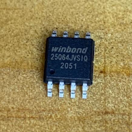
The W25Q64JVSSIQ operates as a serial NOR Flash memory accessed via the SPI bus:
1. SPI Interface Modes: The device supports three interface modes selected by commands. Standard SPI uses four signals (CLK, /CS, DI, DO). Dual SPI uses IO0 and IO1 for bidirectional 2-bit data transfer at 266 MHz equivalent. Quad SPI activates all four I/O pins (IO0-IO3) for 4-bit transfer at 532 MHz equivalent, dramatically reducing code shadowing and XIP access time.
2. Memory Array Access: Read operations begin with a command byte followed by a 24-bit address. In fast read modes, additional dummy clocks allow the pipeline to pre-fetch data. Sequential reads auto-increment the internal address counter within page, sector, or the entire array boundaries. Continuous read mode reduces command overhead to as few as 8 clocks per access.
3. Program and Erase: Page programming writes 1 to 256 bytes at a time. Erase operations support 4 KB sector, 32 KB block, 64 KB block, or full-chip erase. All program and erase operations require a preceding Write Enable (06h) command for safety. A program/erase suspend feature allows interrupting a long operation to read from a different area, then resuming.
4. Write Protection: Multiple protection levels include Status Register write protection (SRWD bit + /WP pin), individual block/sector locking via individual write protect registers, and OTP (One-Time Programmable) security register locking. The /WP pin hardware-protects the status register when SRWD=1.
5. Power Management: The device enters power-down mode via the Power Down (B9h) command, reducing current to <1 uA. Release from power-down takes 3 us typical. On power-up, the device defaults to Standard SPI mode with write disabled.
6. Reset: Both software reset (66h + 99h command sequence) and hardware reset (/RESET pin, available on select packages) restore the device to default state, useful for system recovery.





 English
  简体中文
简体中文  Español
  العربية




