TPS51362RVER


22V 10A sync buck, D-CAP2, 800kHz, 100µA ULQ standby, 0.6-2.0Vout, VQFN-CLIP 28-pin 4.5x3.5mm, -10~85°C

1200

Effective Inventory
Go to Inquiry

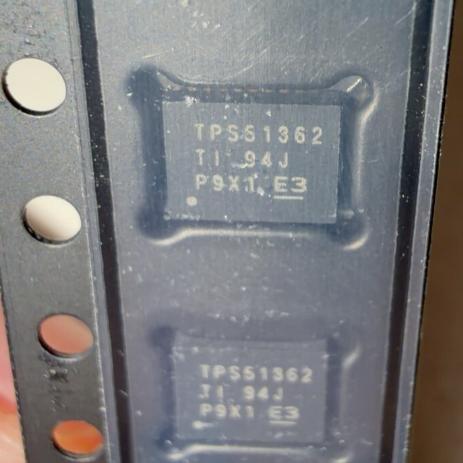
Image for reference only

Manufacturer Part:

TPS51362RVER

Package:

VQFN-CLIP-28 (RVE) (4.5 x 3.5 x 1.0 mm, 0.4mm pitch)

Brand:
Product Categories:
Other recommendations you may be interested in.
Description

The TPS51362RVER from Texas Instruments is a 3-V to 22-V input, 10-A synchronous step-down converter with integrated MOSFETs in a 28-pin VQFN-CLIP package (4.5×3.5 mm, 0.4-mm pitch). It uses TI’s D-CAP2 control topology for compensation-less operation with POSCAP or all-MLCC output capacitors, fixed 800-kHz switching frequency, and ULQ mode drawing only 100 µA in low-power standby. The output voltage is programmable from 0.6 V to 2.0 V via pin-strapping (1.05/1.2/1.35/1.5 V fixed) or resistor divider. Features include programmable soft start, power good, output discharge, and OCL/OVP/UVP/UVLO/thermal shutdown protection. Targeted at DDR VDDQ/VCCIO rails and POL converters in notebook and embedded systems.

The TPS51362RVER is a 10-A integrated-FET synchronous buck converter from Texas Instruments, designed for point-of-load (POL) applications in notebook computers and embedded systems. It operates from a 3-V to 22-V input and produces an adjustable output from 0.6 V to 2.0 V, covering DDR memory VDDQ (1.35 V), VCCIO (1.05 V, 1.2 V), and core logic rails.

The D-CAP2 control topology is the key differentiator. Unlike traditional current-mode or voltage-mode control, D-CAP2 uses adaptive on-time control with internal ripple injection, eliminating the need for Type-II/III compensation components. This simplifies design and supports both POSCAP and all-MLCC output capacitor configurations without stability concerns — a critical advantage in compact designs where MLCCs are preferred for height and reliability.

The ULQ (Ultra-Low Quiescent) mode reduces the bias current to 100 µA when the LP# pin is pulled low, enabling long battery life during system standby. This is a significant improvement over standard auto-skip modes that typically draw 500 µA to 1 mA. In normal PWM mode, the device operates at a fixed 800-kHz frequency, balancing efficiency and inductor size.

The output voltage can be set by pin-strapping REFIN and REFIN2 pins (1.05 V, 1.2 V, 1.35 V, 1.5 V fixed options) without external resistors, or by a resistor divider from the 2.0-V VREF pin for any voltage from 0.6 V to 2.0 V. This flexibility supports multiple DDR generations and rail voltages with a single BOM.

The integrated bootstrap MOSFET switch eliminates the need for an external bootstrap diode. The low-side MOSFET RDS(on) sensing provides temperature-compensated overcurrent protection without an external sense resistor. The VQFN-CLIP-28 package achieves a compact 15.75-mm² footprint with an exposed thermal pad for efficient heat dissipation.

**D-CAP2 Control:** The TPS51362 uses TI’s D-CAP2 (Direct Capacitor-Area-Free 2nd generation) control, which combines adaptive on-time modulation with internal ripple injection. The error amplifier compares FB against an internal reference; the on-time generator produces a fixed-duration pulse (proportional to VIN/VOUT) each switching cycle. Internal ripple injection at FB emulates the inductor current ripple, providing the information needed for stable operation without external compensation. This topology is inherently stable with any output capacitor type (POSCAP, MLCC, or mixed) as long as ESR is above a minimum threshold.

**ULQ Mode:** When LP# is pulled low, the device enters ultra-low-quiescent mode. The controller reduces internal bias currents and switches to a pulse-skip mode where the switching frequency scales with load. At zero load, only 100 µA is drawn from the input supply. The output voltage regulation accuracy degrades slightly in ULQ mode but remains within DDR specification limits.

**Power Stage:** The integrated high-side and low-side MOSFETs are optimized for low duty-cycle operation (3-5 V output from 12-19 V input). The low-side RDS(on) is also used for current sensing — the voltage across the low-side FET during the off-time is measured and temperature-compensated to set the overcurrent limit threshold, eliminating an external sense resistor.

**Bootstrap and Pre-Bias:** The integrated bootstrap switch charges the BOOT capacitor from VDD through an internal MOSFET (not a diode), reducing the BOOT voltage drop and enabling start-up into pre-biased outputs without discharging the load first.

Pin Name Type Description
1 VDD P Internal 5V LDO output and internal supply bypass; connect 1µF ceramic to GND; do not load externally
2 EN I Enable; pull high to enable; has internal pull-up; pull below 0.4V to disable; UVLO threshold ~4.5V on VIN
3 LP# I Low-power mode control; pull low for ULQ mode (100µA Iq); pull high for normal PWM/auto-skip; has internal pull-up
4 PGOOD O Open-drain power-good output; asserts when FB is within ±10% of target; connect external pull-up resistor to logic supply
5 VFB I Voltage feedback input; connect to output voltage divider midpoint or tie to VREF for resistor-less fixed voltage; reference 0.6V
6 VREF O 2.0V reference output; 300µA source capability; bypass with 0.1µF to GND; use for resistor-divider output voltage setting
7 REFIN I Output voltage select pin 1; float or tie to GND during startup to select fixed voltage (see truth table); determines 1.05/1.2/1.5/1.35V
8 REFIN2 I Output voltage select pin 2; same function as REFIN; both pins sampled at startup; latched until next power cycle
9 SS I/O Soft-start programming; connect capacitor to GND; 5µA charge current; larger cap = slower start; leave floating for default 1ms
10 MODE I Operation mode select; controls auto-skip vs forced-PWM behavior; tie to GND or float per datasheet recommendation
11-18 GND G Signal and power ground; connect to PCB ground plane and exposed thermal pad; critical for thermal and electrical performance
19 SW O Switch node; connect to output inductor; high dv/dt; keep copper short to reduce EMI; abs max -1.5V to 24V
20 BOOT I/O Bootstrap capacitor; connect 0.1µF ceramic from BOOT to SW; internal bootstrap switch charges from VDD
21 VIN P Main input supply (3-22V); connect input bypass capacitors (10µF ceramic + bulk) close to pin; high-frequency decoupling critical
22-28 VIN/GND P/G Additional VIN and GND pins for power distribution and thermal relief; follow PCB layout guidelines per datasheet
Application Description
Notebook DDR VDDQ Supply Generate 1.35V DDR3L VDDQ from 5V or 12V system rail; 10A supports 2-DIMM configurations; REFIN/REFIN2 pin-strap sets 1.35V without resistors; ULQ mode maintains standby regulation at 100µA Iq for S3 sleep state; D-CAP2 stable with MLCC-only output
Embedded SoC Core Rail Power 0.8-1.2V core from 5V or 12V intermediate rail; 10A supports mid-range SoCs and FPGAs; resistor divider from VREF sets precise voltage; soft-start controls inrush; PGOOD drives reset logic
SSD Controller Power Convert 5V or 12V to 1.2V core and 1.8V I/O rails; compact VQFN-CLIP footprint fits M.2 SSD form factor; D-CAP2 eliminates compensation components reducing BOM; 100µA ULQ extends laptop battery during idle
Model Manufacturer Compatibility Key Difference
TPS51363RVER TI Pin-Compatible Upgrade Same VQFN-CLIP-28; 12A output (vs 10A); same D-CAP2 control; higher current capability for next-gen platforms
TPS51362ARVER TI Pin-Compatible, Newer A-version with improved jitter and EMI performance; same pinout and electrical specs; recommended for new designs
ISL95813HRTZ Renesas Functional Equivalent 5-25V input; 10A; D-CAP-like R3 modulation; QFN-28 (5x6mm, larger); similar features; use as second source
MP8867GN-Z MPS Competitive Alternative 4.5-22V input; 8A; 800kHz; QFN-20 (3x4mm, smaller); lower current but smaller package; use for space-constrained sub-10A designs
Recommend Parts
PMIC for AM335x, 3 bucks, 2 LDOs, battery charger, WLED, I2C, VQFN-48

Brand:

Package:

VQFN-48 (6×6 mm, 0.4 mm pitch)
In stock:
8909pcs

Cargo cycle: 3~7 Days
The minimum order is 1

Go to Inquiry
Octal D-type flip-flop, edge-triggered, async clear, 28MHz, SOP-20

Brand:

Package:

SOP-20 (NS) (12.6×7.8 mm)
In stock:
8359pcs

Cargo cycle: 3~7 Days
The minimum order is 1

Go to Inquiry
3-to-8 decoder/demux, active-low outputs, 3 enable inputs, 15ns, PDIP-16

Brand:

Package:

PDIP-16 (24.33×9.4 mm, Through-Hole)
In stock:
11952pcs

Cargo cycle: 3~7 Days
The minimum order is 1

Go to Inquiry
2W mono Class-AB audio amp, BTL speaker + SE headphone, 2.5-5.5V, HVSSOP-8

Brand:

Package:

HVSSOP-8 (DGN) (3.0×4.9 mm, PowerPAD)
In stock:
3337pcs

Cargo cycle: 3~7 Days
The minimum order is 1

Go to Inquiry
10/100 Ethernet PHY, MII/RMII/SNI, Auto-MDIX, 270mW, LQFP-48, commercial

Brand:

Package:

LQFP-48 (7×7 mm)
In stock:
14754pcs

Cargo cycle: 3~7 Days
The minimum order is 1

Go to Inquiry
Octal bus transceiver, 3-state outputs, 2-6V, 12ns tpd, TSSOP-20

Brand:

Package:

TSSOP-20 (6.5×6.4 mm)
In stock:
2638pcs

Cargo cycle: 3~7 Days
The minimum order is 1

Go to Inquiry
Quality Assurance

All electronic components we source from our partnered supply chains go through strict incoming inspections.Through careful testing, we ensure everything delivered to customers is genuine original parts and meets quality requirements.In addition, we keep complete inspection records to make the entire supply chain process clear and traceable.

Certification
We have obtained a number of professional certifications and built our own professional testing laboratory.This ensures that every product we deliver to our customers meets the highest quality requirements.We conduct tests in strict accordance with procedures to ensure stable product quality and accurate parameters.To guarantee genuine original parts, we also cooperate with reliable third-party testing institutions for strict quality inspection.We always attach great importance to quality and fully comply with industry standards, relevant regulations, and ISO 9001:2015 requirements.

Shipping & Payment

All electronic components we source from our partnered supply chains go through strict incoming inspections.Through careful testing, we ensure everything delivered to customers is genuine original parts and meets quality requirements.In addition, we keep complete inspection records to make the entire supply chain process clear and traceable.

Certification
We have obtained a number of professional certifications and built our own professional testing laboratory.This ensures that every product we deliver to our customers meets the highest quality requirements.We conduct tests in strict accordance with procedures to ensure stable product quality and accurate parameters.To guarantee genuine original parts, we also cooperate with reliable third-party testing institutions for strict quality inspection.We always attach great importance to quality and fully comply with industry standards, relevant regulations, and ISO 9001:2015 requirements.

Service & Packaging

All electronic components we source from our partnered supply chains go through strict incoming inspections.Through careful testing, we ensure everything delivered to customers is genuine original parts and meets quality requirements.In addition, we keep complete inspection records to make the entire supply chain process clear and traceable.

Certification
We have obtained a number of professional certifications and built our own professional testing laboratory.This ensures that every product we deliver to our customers meets the highest quality requirements.We conduct tests in strict accordance with procedures to ensure stable product quality and accurate parameters.To guarantee genuine original parts, we also cooperate with reliable third-party testing institutions for strict quality inspection.We always attach great importance to quality and fully comply with industry standards, relevant regulations, and ISO 9001:2015 requirements.









