Home > Integrated Circuits ICs > PIC18F67K40-I/PT

PIC18F67K40-I/PT


PIC18 8-bit MCU, 128KB Flash, 3562B RAM, 1KB EEPROM, 60 I/O, 47-ch 10-bit ADC, 5x EUSART, XLP, 64-TQFP, -40~85C

8420

Effective Inventory
Go to Inquiry

Image for reference only

Manufacturer Part:

PIC18F67K40-I/PT

Package:

64-Lead TQFP (PT Package) (10 x 10 x 1.2 mm, 0.5mm pitch)

Brand:
Other recommendations you may be interested in.
Description

The PIC18F67K40-I/PT from Microchip Technology is a 64-pin, low-power, high-performance 8-bit microcontroller with XLP (eXtreme Low Power) technology in a 64-lead TQFP package (10x10mm, 0.5mm pitch). Key features: PIC18 enhanced core at up to 64MHz (16 MIPS), 128KB Flash program memory, 3562 bytes SRAM, 1024 bytes EEPROM, 60 I/O pins, 47-channel 10-bit ADC, 1x 5-bit DAC, 3 comparators, 2x I2C/SPI, 5x EUSART with LIN, 5x 8-bit timers, 4x 16-bit timers, 2x standalone 10-bit PWM, 5x CCP modules, 1x Complementary Waveform Generator (CWG), 1x Zero-Cross Detect (ZCD), 1x CRC with Memory Scan, 2x Signal Measurement Timer (SMT), 1x Hardware Limit Timer (HLT), Windowed Watchdog Timer (WWDT), Peripheral Pin Select (PPS), Hardware Capacitive Voltage Divider (CVD) for mTouch. Operating voltage: 2.3V to 5.5V (LF variant: 1.8V to 3.6V). XLP: Sleep mode 50nA @ 1.8V, Active mode 32uA/MHz @ 1.8V. Industrial temperature range: -40C to 85C. Functional safety ready (IEC 61508, ISO 26262). RoHS compliant.

The PIC18F67K40-I/PT from Microchip Technology is a 64-pin, high-performance 8-bit microcontroller from the PIC18 K40 family, featuring eXtreme Low Power (XLP) technology. The device combines large memory resources with an extensive peripheral set in a compact 64-lead TQFP package, targeting general-purpose embedded control applications that require rich analog integration, flexible communication interfaces, and low power consumption.

The PIC18 K40 family represents a significant evolution over the classic PIC18F series, introducing Core Independent Peripherals (CIPs) that can operate without CPU intervention, reducing CPU overhead and enabling more efficient system designs. Key CIPs include the Complementary Waveform Generator (CWG) for half-bridge and full-bridge motor drive, the CRC with Memory Scan for data integrity verification, the Hardware Capacitive Voltage Divider (CVD) for capacitive touch sensing, and the Signal Measurement Timer (SMT) for precise pulse and period measurements.

Memory resources are substantial: 128KB of Flash program memory (supporting self read/write for bootloader and data logging), 3562 bytes of SRAM (sufficient for complex data buffering and DSP algorithms), and 1024 bytes of data EEPROM (for calibration data and configuration parameters that must survive power cycles). The 128KB Flash can hold approximately 65,000 instructions, providing ample space for complex application code.

Analog capabilities are extensive: a 47-channel 10-bit ADC with multiple acquisition modes (including Hardware CVD for touch sensing), a 5-bit DAC for voltage reference generation or simple analog output, 3 analog comparators with configurable hysteresis, and a Fixed Voltage Reference (FVR) module providing 1.024V, 2.048V, and 4.096V reference levels. The Hardware CVD (Capacitive Voltage Divider) enables mTouch capacitive sensing without external components, supporting buttons, sliders, and wheels.

Communication interfaces include 5 EUSART modules with LIN bus support (ideal for automotive and industrial networking), 2 independent I2C/SPI modules (supporting both master and slave modes), and Peripheral Pin Select (PPS) that allows flexible remapping of digital peripheral functions to any of the 60 I/O pins. PPS dramatically simplifies PCB layout by allowing signals to be routed to the most convenient pins.

Timer resources include 5 x 8-bit timers, 4 x 16-bit timers, 2 x Signal Measurement Timers (SMT) for pulse width, period, and duty cycle measurement, and 1 x Hardware Limit Timer (HLT) that can generate periodic interrupts even in Sleep mode. PWM outputs include 2 standalone 10-bit PWM modules and 5 CCP (Capture/Compare/PWM) modules.

XLP technology enables extremely low power consumption: Sleep mode draws only 50nA at 1.8V (typical), Active mode draws 32uA/MHz at 1.8V, and the Low-Power Brown-Out Reset (LPBOR) consumes minimal current. The device supports multiple power-saving modes: Sleep (CPU and most peripherals stopped), Idle (CPU stopped, selected peripherals running), and Doze (CPU clock divided down, peripherals at full speed).

The -I/PT suffix indicates: I = Industrial temperature range (-40C to 85C); PT = 64-lead TQFP package. An Extended temperature variant (-E/PT, -40C to 125C) is also available for automotive applications. The device is functional safety ready, with documentation (FMEDA report and Safety Manual) available on request for IEC 61508 and ISO 26262 certifications.
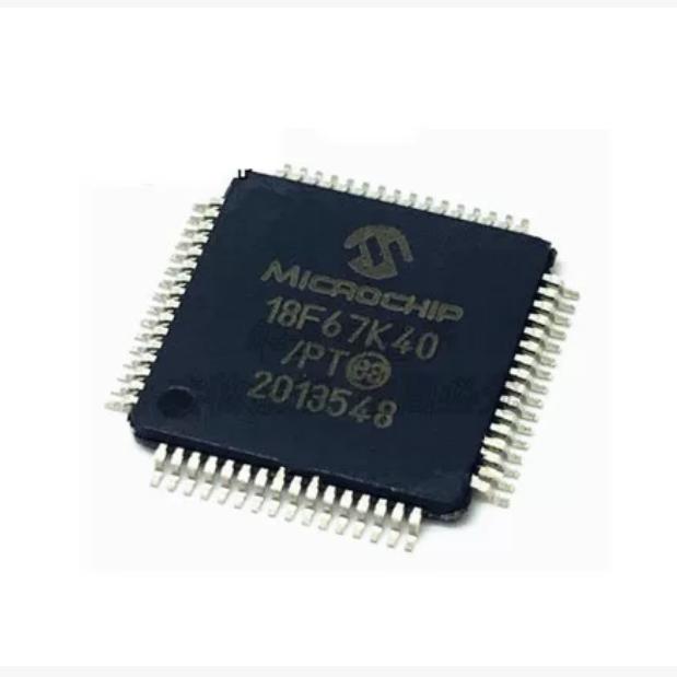

The PIC18F67K40-I/PT operates as an enhanced 8-bit PIC18 microcontroller with XLP technology and Core Independent Peripherals.

PIC18 Enhanced Core: The CPU implements the PIC18 enhanced instruction set with 83 instructions (up from 75 in classic PIC18), supporting 31 levels of hardware stack. The instruction word is 16 bits wide, and most instructions execute in a single cycle (2 clock periods). At the maximum 64MHz internal oscillator frequency, instruction execution rate is 16 MIPS. The core includes an 8×8 hardware multiplier for single-cycle multiplication, and supports both direct and indirect addressing with access RAM for fast variable access.

Oscillator Module: The internal oscillator block provides a 64MHz high-frequency oscillator (HFINTOSC) and a 64kHz low-frequency oscillator (LFINTOSC), eliminating the need for external crystals in most applications. The HFINTOSC can be tuned via the OSCTUNE register for precise timing. External oscillator modes (EC, LP, XT, HS) are also supported for applications requiring crystal accuracy. A Fail-Safe Clock Monitor (FSCM) detects external oscillator failure and automatically switches to the internal oscillator.

Peripheral Pin Select (PPS): The PPS module allows most digital peripheral input and output functions to be mapped to any of the available I/O pins through software configuration. This eliminates the pin-function constraints of fixed-peripheral devices and dramatically simplifies PCB routing. Each digital peripheral (UART TX/RX, SPI SCK/SDI/SDO, I2C SDA/SCL, CCP output, PWM output, etc.) has a corresponding PPS output or input selection register.

Core Independent Peripherals (CIPs): CIPs can operate autonomously without CPU intervention, enabling the device to handle complex real-time tasks with minimal software overhead. Key CIPs include: (1) CWG (Complementary Waveform Generator) – generates complementary PWM signals with programmable dead band for half-bridge and full-bridge motor drive; (2) CRC with Memory Scan – performs CRC calculations on Flash and RAM for data integrity; (3) SMT (Signal Measurement Timer) – measures pulse width, period, and duty cycle of external signals with 16-bit or 32-bit resolution; (4) HLT (Hardware Limit Timer) – generates periodic interrupts even in Sleep mode for wake-up timing; (5) ZCD (Zero-Cross Detect) – detects AC line zero crossings for TRIAC dimming and power control.

Hardware CVD (Capacitive Voltage Divider): The CVD module enables capacitive touch sensing using the ADC without external components. It works by charging an internal sample capacitor and then connecting it to an external sensor pad through a voltage divider, measuring the charge transfer. The CVD can detect capacitance changes as small as a few picofarads, sufficient for finger touch detection on buttons, sliders, and wheels.

XLP Power Management: The XLP architecture minimizes power consumption through: (1) Optimized transistor-level design for low leakage; (2) Multiple power domains that can be independently enabled/disabled; (3) Low-Power BOR (LPBOR) that monitors VDD at microamp current levels; (4) Sleep mode (50nA) where the CPU and most peripherals are stopped but selected peripherals (WDT, RTCC, SMT) can continue operating; (5) Idle mode where the CPU is stopped but enabled peripherals continue; (6) Doze mode where the CPU clock is divided down (by 1 to 128) while peripheral clocks remain at full speed, reducing CPU power consumption during less compute-intensive periods.

ADC Module: The 10-bit ADC supports 47 input channels with multiple acquisition modes: individual channel, continuous acquisition, and CVD mode. The ADC can be triggered by multiple sources including timers, PWM events, and software. The conversion time is approximately 2us at the maximum acquisition rate, providing up to 500Ksps throughput. The FVR module provides stable voltage references for accurate ADC measurements independent of VDD variations.

Functional Safety: The device is designed to support functional safety applications per IEC 61508 (industrial) and ISO 26262 (automotive). Key safety features include: CRC/Memory Scan for detecting Flash and RAM corruption, Windowed Watchdog Timer (WWDT) for detecting software hangs, Clock Fail-Safe Monitor (FSCM) for detecting oscillator failures, and Brown-Out Reset (BOR) for detecting supply voltage drops. Microchip provides FMEDA reports and Safety Manuals on request.

Pin Name Type Description
1 RE1 I/O Port E bit 1; general-purpose I/O; PPS capable; can be remapped to digital peripheral functions
2 RE0 I/O Port E bit 0; general-purpose I/O; PPS capable
3 RG0 I/O Port G bit 0; general-purpose I/O; PPS capable
4 RG1 I/O Port G bit 1; general-purpose I/O; PPS capable
5 RG2 I/O Port G bit 2; general-purpose I/O; PPS capable
6 RG3 I/O Port G bit 3; general-purpose I/O; PPS capable
7 VPP/MCLR/RG5 Input/I/O Master Clear (reset) input; active LOW; also serves as VPP during programming; internal pull-up; can be configured as RG5 digital I/O via MCLRE configuration bit
8 RG4 I/O Port G bit 4; general-purpose I/O; PPS capable
9 VSS Power Ground; connect all VSS pins together to system ground plane
10 VDD Power Positive supply; 2.3V to 5.5V; decouple with 0.1uF ceramic capacitor to VSS; connect all VDD pins together
11-16 RF7-RF2 I/O Port F bits 7-2; general-purpose I/O; PPS capable; each pin individually configurable as input or output
17-22 RC2-RC7 I/O Port C bits 2-7; general-purpose I/O; PPS capable; alternate functions include EUSART, SPI, I2C, CCP, PWM depending on PPS configuration
23-28 RD7-RD2 I/O Port D bits 7-2; general-purpose I/O; PPS capable
29-32 RD1-RD0,RC1,RC0 I/O Port D bits 1-0 and Port C bits 1-0; general-purpose I/O; PPS capable
33-40 RA0-RA7 I/O Port A bits 0-7; mixed analog and digital I/O; RA0-RA3 serve as ADC inputs; RA5 can be T0CKI; RA6 and RA7 can be oscillator pins; PPS capable on digital functions
41-48 RB0-RB7 I/O Port B bits 0-7; general-purpose I/O; PPS capable; RB0-RB7 have interrupt-on-change capability; RB5 also serves as ICSP programming clock (PGC); RB6 as ICSP data (PGD)
49-53 RE2,RD3-RD6 I/O Port E bit 2 and Port D bits 3-6; general-purpose I/O; PPS capable
54-56 RF0-RF1,RD0 I/O Port F bits 0-1 and Port D bit 0; general-purpose I/O; PPS capable
57 RF3 I/O Port F bit 3; PPS capable; also SCL2/SDA2 alternate when configured
58 RF4 I/O Port F bit 4; PPS capable
59 RF5 I/O Port F bit 5; PPS capable
60 RB5/PGC I/O Port B bit 5; also ICSP programming clock; interrupt-on-change capable
61 RB4 I/O Port B bit 4; interrupt-on-change capable; PPS capable
62 RB3 I/O Port B bit 3; PPS capable
63 RB2 I/O Port B bit 2; PPS capable
64 RB1 I/O Port B bit 1; PPS capable
Application Description
Industrial Automation and Control 128KB Flash and rich peripheral set support complex PLC logic, PID control loops, and multi-protocol communication; 5x EUSART with LIN suits industrial networks; CRC/Memory Scan ensures code integrity; functional safety documentation available for SIL-certified systems
Capacitive Touch User Interfaces Hardware CVD module enables mTouch capacitive sensing for buttons, sliders, and wheels without external touch IC; 47 ADC channels provide ample sensing inputs; PPS simplifies touch sensor PCB routing; XLP Sleep mode extends battery life in portable devices
Motor Control and Power Conversion CWG generates complementary PWM with programmable dead band for half-bridge/full-bridge motor drive; 10-bit ADC monitors motor current and voltage; ZCD enables TRIAC-based AC motor speed control; CCP modules provide additional PWM outputs for multi-axis control
Smart Metering and Energy Monitoring 10-bit ADC with FVR provides accurate voltage and current measurement; SMT measures pulse width from energy sensors; EUSART with LIN supports smart meter communication protocols; EEPROM stores calibration data; XLP extends battery life in gas/water meters
Automotive Body Electronics 5V operation and wide temperature range suit automotive environment; LIN bus support via 5x EUSART for body control networks; functional safety ready for ISO 26262 certification; CWG for LED lighting control; extended temperature variant (-40C to 125C) available
Model Manufacturer Compatibility Key Difference
PIC18F47K40-I/PT Microchip Same Family, Fewer Pins 44-pin TQFP variant; same 128KB Flash and peripherals; fewer I/O pins (35 vs 60); fewer ADC channels; smaller package; use when 64-pin I/O count is not needed
PIC18F67K22-I/PT Microchip Previous Generation 64-pin PIC18 K22 family; 128KB Flash; different peripheral mix (no CVD, no CRC, no SMT, no PPS); more mature but fewer Core Independent Peripherals; different register set
PIC18LF67K40-I/PT Microchip Low-Voltage Variant Same as PIC18F67K40 but wider voltage range (1.8V-3.6V for LF vs 2.3V-5.5V for F); use for 3.3V and lower voltage designs; lower maximum operating frequency at reduced voltage
ATmega640-16AU Microchip Alternative Architecture 64-pin TQFP AVR; 64KB Flash; 4KB SRAM; 4KB EEPROM; 16 ADC channels; 4x UART; different instruction set (AVR RISC); requires code rewrite from PIC
STM32F103VBT6 ST 32-bit Alternative 32-bit ARM Cortex-M3; 128KB Flash; 20KB RAM; far more processing power; 72MHz; different architecture; requires ARM development tools; for applications needing 32-bit performance
Recommend Parts
Dual 12-bit DAC, SPI, 2.7-5.5V, 4.5us settling, SOIC-14, AEC-Q100

Brand:

Package:

SOIC-14 (8.65 x 3.9 x 1.5 mm)
In stock:
6368pcs

Cargo cycle: 3~7 Days
The minimum order is 1

Go to Inquiry
14-pin 8-bit PIC MCU, 1792B Flash, 128B SRAM, 10-bit ADC, PDIP-14, industrial

Brand:

Package:

PDIP-14 (19.18 x 6.35 mm)
In stock:
5620pcs

Cargo cycle: 3~7 Days
The minimum order is 1

Go to Inquiry
4Mbit (512Kx8) Multi-Purpose Flash, 2.7-3.6V, 70ns, PLCC-32, SuperFlash

Brand:

Package:

PLCC-32 (11.43 x 13.21 mm)
In stock:
330pcs

Cargo cycle: 3~7 Days
The minimum order is 1

Go to Inquiry
8-bit AVR MCU, 20 MHz, 32KB Flash, 2KB SRAM, TQFP-32, 1.8-5.5V

Brand:

Package:

TQFP-32 (7 x 7 x 1.0 mm)
In stock:
13892pcs

Cargo cycle: 3~7 Days
The minimum order is 1

Go to Inquiry
E1/T1 Line Interface Unit, 8.192Mbps, short/long haul, integrated CDR, 80-MQFP, 3.3V

Brand:

Package:

80-MQFP (14x14mm)
In stock:
14099pcs

Cargo cycle: 3~7 Days
The minimum order is 1

Go to Inquiry
ARM7TDMI MCU, 55MHz, 256KB Flash, 64KB SRAM, Ethernet MAC, USB, CAN, LQFP-100

Brand:

Package:

LQFP-100
In stock:
3752pcs

Cargo cycle: 3~7 Days
The minimum order is 1

Go to Inquiry
Quality Assurance

All electronic components we source from our partnered supply chains go through strict incoming inspections.Through careful testing, we ensure everything delivered to customers is genuine original parts and meets quality requirements.In addition, we keep complete inspection records to make the entire supply chain process clear and traceable.

Certification
We have obtained a number of professional certifications and built our own professional testing laboratory.This ensures that every product we deliver to our customers meets the highest quality requirements.We conduct tests in strict accordance with procedures to ensure stable product quality and accurate parameters.To guarantee genuine original parts, we also cooperate with reliable third-party testing institutions for strict quality inspection.We always attach great importance to quality and fully comply with industry standards, relevant regulations, and ISO 9001:2015 requirements.

Shipping & Payment

All electronic components we source from our partnered supply chains go through strict incoming inspections.Through careful testing, we ensure everything delivered to customers is genuine original parts and meets quality requirements.In addition, we keep complete inspection records to make the entire supply chain process clear and traceable.

Certification
We have obtained a number of professional certifications and built our own professional testing laboratory.This ensures that every product we deliver to our customers meets the highest quality requirements.We conduct tests in strict accordance with procedures to ensure stable product quality and accurate parameters.To guarantee genuine original parts, we also cooperate with reliable third-party testing institutions for strict quality inspection.We always attach great importance to quality and fully comply with industry standards, relevant regulations, and ISO 9001:2015 requirements.

Service & Packaging

All electronic components we source from our partnered supply chains go through strict incoming inspections.Through careful testing, we ensure everything delivered to customers is genuine original parts and meets quality requirements.In addition, we keep complete inspection records to make the entire supply chain process clear and traceable.

Certification
We have obtained a number of professional certifications and built our own professional testing laboratory.This ensures that every product we deliver to our customers meets the highest quality requirements.We conduct tests in strict accordance with procedures to ensure stable product quality and accurate parameters.To guarantee genuine original parts, we also cooperate with reliable third-party testing institutions for strict quality inspection.We always attach great importance to quality and fully comply with industry standards, relevant regulations, and ISO 9001:2015 requirements.









