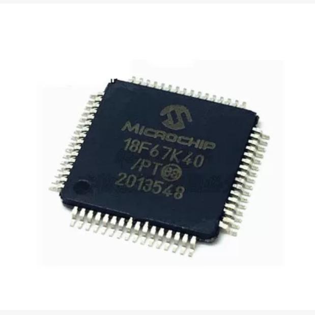
The PIC18F67K40-I/PT from Microchip Technology is a 64-pin, high-performance 8-bit microcontroller from the PIC18 K40 family, featuring eXtreme Low Power (XLP) technology. The device combines large memory resources with an extensive peripheral set in a compact 64-lead TQFP package, targeting general-purpose embedded control applications that require rich analog integration, flexible communication interfaces, and low power consumption.
The PIC18 K40 family represents a significant evolution over the classic PIC18F series, introducing Core Independent Peripherals (CIPs) that can operate without CPU intervention, reducing CPU overhead and enabling more efficient system designs. Key CIPs include the Complementary Waveform Generator (CWG) for half-bridge and full-bridge motor drive, the CRC with Memory Scan for data integrity verification, the Hardware Capacitive Voltage Divider (CVD) for capacitive touch sensing, and the Signal Measurement Timer (SMT) for precise pulse and period measurements.
Memory resources are substantial: 128KB of Flash program memory (supporting self read/write for bootloader and data logging), 3562 bytes of SRAM (sufficient for complex data buffering and DSP algorithms), and 1024 bytes of data EEPROM (for calibration data and configuration parameters that must survive power cycles). The 128KB Flash can hold approximately 65,000 instructions, providing ample space for complex application code.
Analog capabilities are extensive: a 47-channel 10-bit ADC with multiple acquisition modes (including Hardware CVD for touch sensing), a 5-bit DAC for voltage reference generation or simple analog output, 3 analog comparators with configurable hysteresis, and a Fixed Voltage Reference (FVR) module providing 1.024V, 2.048V, and 4.096V reference levels. The Hardware CVD (Capacitive Voltage Divider) enables mTouch capacitive sensing without external components, supporting buttons, sliders, and wheels.
Communication interfaces include 5 EUSART modules with LIN bus support (ideal for automotive and industrial networking), 2 independent I2C/SPI modules (supporting both master and slave modes), and Peripheral Pin Select (PPS) that allows flexible remapping of digital peripheral functions to any of the 60 I/O pins. PPS dramatically simplifies PCB layout by allowing signals to be routed to the most convenient pins.
Timer resources include 5 x 8-bit timers, 4 x 16-bit timers, 2 x Signal Measurement Timers (SMT) for pulse width, period, and duty cycle measurement, and 1 x Hardware Limit Timer (HLT) that can generate periodic interrupts even in Sleep mode. PWM outputs include 2 standalone 10-bit PWM modules and 5 CCP (Capture/Compare/PWM) modules.
XLP technology enables extremely low power consumption: Sleep mode draws only 50nA at 1.8V (typical), Active mode draws 32uA/MHz at 1.8V, and the Low-Power Brown-Out Reset (LPBOR) consumes minimal current. The device supports multiple power-saving modes: Sleep (CPU and most peripherals stopped), Idle (CPU stopped, selected peripherals running), and Doze (CPU clock divided down, peripherals at full speed).
The -I/PT suffix indicates: I = Industrial temperature range (-40C to 85C); PT = 64-lead TQFP package. An Extended temperature variant (-E/PT, -40C to 125C) is also available for automotive applications. The device is functional safety ready, with documentation (FMEDA report and Safety Manual) available on request for IEC 61508 and ISO 26262 certifications.





 English
  简体中文
简体中文  Español
  العربية