TPS54360DDAR


60V 3.5A 降压型 DC-DC,92mΩ MOSFET,146µA Iq Eco 模式,100kHz-2.5MHz,可调 UVLO,HSOIC-8 PowerPAD,-40~125°C

8000

有效库存
转到查询

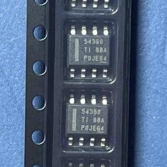
Image for reference only

制造商零件:

TPS54360DDAR

包装:

带 PowerPAD 的 HSOIC-8(DDA)(4.9 x 6.0 x 1.5 毫米,1.27 毫米间距)

品牌:
您可能感兴趣的其他建议.
说明

The TPS54360DDAR from Texas Instruments is a 60-V, 3.5-A step-down DC-DC converter with an integrated 92-mΩ high-side MOSFET in an 8-pin HSOIC PowerPAD package. It features a wide 4.5-V to 60-V input range (65-V abs max), adjustable output from 0.8 V to 58.8 V, current-mode control with 100-kHz to 2.5-MHz programmable switching frequency, Eco-mode pulse skipping for 146-µA quiescent current at light load, external clock synchronization, adjustable UVLO, internal soft start, and comprehensive protection (cycle-by-cycle current limit, thermal shutdown, overvoltage, frequency foldback). Target applications include 12-V/24-V/48-V industrial, automotive, and communications power systems.

The TPS54360DDAR is a 60-V, 3.5-A step-down DC-DC converter from Texas Instruments with an integrated high-side N-channel MOSFET (92 mΩ). It is designed for 12-V, 24-V, and 48-V industrial, automotive, and communications power systems where a compact, efficient, wide-input-range buck converter is needed.

The device uses peak current-mode control, which simplifies external loop compensation and provides predictable transient response. The switching frequency is programmable from 100 kHz to 2.5 MHz via a single external resistor on the RT/CLK pin, allowing designers to trade off efficiency versus inductor size. An external clock can also drive the RT/CLK pin for synchronization with other converters in the system.

At light loads, the Eco-mode pulse-skipping operation reduces the quiescent current to 146 µA (typical), significantly extending battery life in always-on or standby applications. In shutdown (EN pin low), the supply current drops to 2 µA. The internal BOOT recharge FET maintains low dropout at light loads without requiring an external bootstrap capacitor refresh.

The adjustable UVLO threshold (default 4.3 V rising) can be raised using two external resistors on the EN pin with built-in hysteresis current (3.4 µA typ), enabling precise power-up sequencing. Internal soft start (1.5 ms at 500 kHz) prevents inrush current and output overshoot.

Protection features include accurate cycle-by-cycle current limit (5.5 A typ), thermal shutdown (176°C), output overvoltage protection, and frequency foldback during overload. The device survives automotive load dump pulses up to 65 V per ISO 7637.

The HSOIC-8 PowerPAD package provides a low junction-to-case thermal resistance (3.6°C/W θJCbot) and is rated for operation from -40°C to 125°C ambient (150°C junction). The PowerPAD must be soldered to the PCB ground plane for proper thermal performance.

**Power Stage and Current-Mode Control:** The TPS54360 integrates a high-side N-channel MOSFET (92 mΩ) and operates as a peak current-mode buck converter. The error amplifier compares the FB pin voltage with the 0.8-V internal reference and drives the COMP pin. The PWM comparator compares the COMP voltage with the sensed switch current to determine the on-time. Current-mode control provides inherent line rejection, cycle-by-cycle current limiting, and simple Type-II compensation.

**Eco-mode (Pulse Skip):** When the load current drops below the pulse-skip threshold, the converter enters Eco-mode. The high-side MOSFET stops switching and the output coasts down until FB falls below the reference, at which point a single pulse is delivered. This eliminates continuous switching losses, reducing quiescent current to 146 µA. The BOOT recharge FET ensures the bootstrap capacitor stays charged during skip mode.

**Frequency and Synchronization:** The switching frequency is set by an external resistor from RT/CLK to GND (200 kΩ = 500 kHz). An external clock on RT/CLK overrides the resistor setting; the internal PLL locks within 78 µs. Frequency foldback reduces the switching frequency to 1/4 of the set value during overcurrent, reducing MOSFET thermal stress.

**UVLO and Enable:** The EN pin serves dual purpose: pulling it below 1.2 V shuts down the converter (2 µA Iq), while external resistors set a custom UVLO threshold. The internal 3.4-µA hysteresis current source creates programmable UVLO hysteresis without a third resistor.

**Protection:** Cycle-by-cycle current limit (5.5 A) protects the MOSFET. Thermal shutdown at 176°C with 12°C hysteresis. OVP on the FB pin triggers if output exceeds 109% of set point. Frequency foldback activates during sustained overcurrent.

针脚 名称 类型 说明
1 BOOT 输入/输出 Bootstrap capacitor connection; connect 0.1µF ceramic from BOOT to SW; internal BOOT recharge FET keeps capacitor charged during skip mode
2 VIN P Input supply pin (4.5-60V); connect to input bypass capacitors (0.1µF ceramic + 10µF ceramic placed close to pin); internal UVLO threshold 4.3V
3 EN I Enable and UVLO adjust; float or pull above 1.2V to enable; pull below 1.2V to shutdown; add two resistors from VIN to EN to GND to set custom UVLO threshold with built-in 3.4µA hysteresis
4 RT/CLK I Switching frequency set resistor or external clock input; connect resistor to GND (200kΩ=500kHz, range 100kHz-2.5MHz); external clock overrides resistor; do not leave floating
5 FB I Feedback input; connect to output voltage divider (Rtop from VOUT to FB, Rbot from FB to GND); Vref=0.8V; divider sets output voltage; place divider close to pin
6 COMP 输入/输出 Error amplifier output; connect Type-II compensation network (Rcomp, Ccomp, Chf) from COMP to GND; compensation sets loop bandwidth and phase margin
7 接地 P Signal and power ground; connect to PCB ground plane; PowerPAD on package bottom must be soldered to ground plane for thermal dissipation
8 SW O Switch node; connects to output inductor; high-frequency switching node (keep copper area minimal to reduce EMI); absolute max -1V to 65V
垫子 PowerPAD P Thermal pad; must be soldered to PCB ground plane; θJCbot=3.6°C/W; critical for thermal performance at high power dissipation
应用 说明
Automotive 12V/24V Power Supply Convert 12V or 24V battery to 5V/3.3V for MCU, CAN transceiver, and sensor rails; 60V input withstands load dump; Eco-mode minimizes standby battery drain; adjustable UVLO prevents deep battery discharge; AEC-Q100 variant TPS54360-Q1 available
Industrial 24V/48V Bus Converter Step down 24V or 48V industrial supply to intermediate 12V or 5V rail; wide input range handles bus voltage transients; 3.5A output powers multiple downstream loads; external sync aligns switching with other converters to avoid beat frequencies
Telecom 48V to Point-of-Load Derive POL rails (1.2V, 1.8V, 3.3V) from -48V telecom bus (use positive 48V rail); high efficiency reduces thermal load in enclosed equipment; programmable frequency optimizes inductor selection for space-constrained boards
Battery-Powered Always-On System Regulate 4S-13S Li-Ion pack (14.4-54.6V) to 5V or 3.3V for IoT gateway; 146µA Eco-mode Iq extends battery life during sleep; 2µA shutdown current enables deep-sleep power gating; EN pin controlled by MCU for on-demand power
模型 制造商 兼容性 主要区别
TPS54560DDAR TI 针脚兼容升级 Same HSOIC-8 pinout; 5A output (vs 3.5A); same 60V input; same features; drop-in for higher current needs
LM5141DDAR TI 功能等效 60V 3.5A buck controller (external MOSFET); higher efficiency at heavy load; more external components; use when optimal MOSFET selection is needed
MAX17552ATB+ ADI 竞争性替代方案 60V 1A buck (lower current); internal MOSFET; 2.2MHz; TDFN-10; smaller footprint; use for lower-current 60V applications
TPS54360BDDAR TI 系列升级 Newer B-version; improved EMI; same pinout and electrical specs; recommended for new designs
推荐部件
3-16S battery monitor/protector, Li-Ion/LiFePO4, 2 ADCs, TQFP-48

品牌:

封装:

TQFP-48 (7 x 7 x 1.0 mm)
有库存:
2150pcs

货运周期:3~7 天
最低订购量为 1

转到查询
I2C 4.5A 1-cell Li-ion charger, NVDC power path, USB OTG, VQFN-24

品牌:

封装:

VQFN-24 (4.0 x 4.0 x 0.75 mm, with thermal pad)
有库存:
4182pcs

货运周期:3~7 天
最低订购量为 1

转到查询
Single micropower RRIO op-amp, 2.7-10V, 65kHz, 11uA, SOT-23-5

品牌:

封装:

SOT-23-5 (2.9 x 2.8 x 1.15 mm)
有库存:
8750pcs

货运周期:3~7 天
最低订购量为 1

转到查询
Single 2-input AND gate, 1.65-5.5V, 24mA drive, SOT-23-5, LVC

品牌:

封装:

SOT-23-5 (2.9 x 1.6 x 1.15 mm)
有库存:
35000 件

货运周期:3~7 天
最低订购量为 1

转到查询
8-bit parallel-load shift register, PISO, 2-6V, 24 MHz, SOIC-16

品牌:

封装:

SOIC-16 (9.9 x 6.0 mm)
有库存:
4837pcs

货运周期:3~7 天
最低订购量为 1

转到查询
Quad differential line receiver, EIA-422/423, 3-state TTL outputs, 5V, SOIC-16

品牌:

封装:

SOIC-16 (9.9 x 6.0 mm)
有库存:
0 件

货运周期:3~7 天
最低订购量为 1

转到查询
质量保证

我们从合作供应链采购的所有电子元件都经过严格的进货检验。通过仔细的测试,我们确保交付给客户的所有产品都是原装正品,符合质量要求。此外,我们还保存完整的检验记录,使整个供应链流程清晰可查。.

认证
我们获得了多项专业认证,并建立了自己的专业检测实验室,确保交付给客户的每一件产品都符合最高质量要求。我们严格按照流程进行检测,确保产品质量稳定、参数准确。为保证原装正品,我们还与可靠的第三方检测机构合作,进行严格的质量检测。我们始终高度重视质量,完全符合行业标准、相关法规和 ISO 9001:2015 的要求。.

发货与付款

我们从合作供应链采购的所有电子元件都经过严格的进货检验。通过仔细的测试,我们确保交付给客户的所有产品都是原装正品,符合质量要求。此外,我们还保存完整的检验记录,使整个供应链流程清晰可查。.

认证
我们获得了多项专业认证,并建立了自己的专业检测实验室,确保交付给客户的每一件产品都符合最高质量要求。我们严格按照流程进行检测,确保产品质量稳定、参数准确。为保证原装正品,我们还与可靠的第三方检测机构合作,进行严格的质量检测。我们始终高度重视质量,完全符合行业标准、相关法规和 ISO 9001:2015 的要求。.

服务与包装

我们从合作供应链采购的所有电子元件都经过严格的进货检验。通过仔细的测试,我们确保交付给客户的所有产品都是原装正品,符合质量要求。此外,我们还保存完整的检验记录,使整个供应链流程清晰可查。.

认证
我们获得了多项专业认证,并建立了自己的专业检测实验室,确保交付给客户的每一件产品都符合最高质量要求。我们严格按照流程进行检测,确保产品质量稳定、参数准确。为保证原装正品,我们还与可靠的第三方检测机构合作,进行严格的质量检测。我们始终高度重视质量,完全符合行业标准、相关法规和 ISO 9001:2015 的要求。.



