TPS5430DDAR


3A、36V 降压型 DC-DC 转换器,500 kHz,SO PowerPAD-8

0

有效库存
转到查询

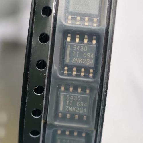
Image for reference only

制造商零件:

TPS5430DDAR

包装:

8-SO PowerPAD(HSOIC-8,5 x 4 x 1.55 毫米)

品牌:
您可能感兴趣的其他建议.
说明

"(《世界人权宣言》) TPS5430DDAR by Texas Instruments is a 3A step-down DC-DC converter with a wide 5.5V to 36V input range and adjustable output from 1.22V to 31V. It integrates a 100 mOhm high-side MOSFET for up to 95% efficiency, with a fixed 500 kHz switching frequency enabling small external filter components. Internal compensation eliminates external loop components, and input voltage feedforward ensures stable transient response across the full input range.

Protection features include cycle-by-cycle current limiting, overvoltage protection, UVLO, and thermal shutdown. The ENA pin provides on/off control (15 uA shutdown Iq), and internal slow start (8 ms) limits inrush current. Packaged in 8-SO PowerPAD (HSOIC-8) with exposed thermal pad, operating from -40 to +125C junction. MSL-2, lead-free, RoHS/REACH compliant. ECCN EAR99. Active. Ideal for 24V industrial bus conversion, automotive power, and embedded supplies.

The TPS5430DDAR is a 3A step-down (buck) DC-DC converter manufactured by Texas Instruments, part of the SWIFT family. It features a wide input voltage range of 5.5V to 36V with an adjustable output voltage from 1.22V to 31V, set via an external resistor divider with 1.5% initial reference accuracy. The device integrates a 100 mOhm high-side N-channel MOSFET switch, achieving up to 95% efficiency.

The fixed 500 kHz switching frequency enables use of small external inductors and capacitors, minimizing solution footprint. Internal compensation simplifies design by eliminating external compensation network components. An input voltage feedforward circuit improves line regulation and transient response across the wide input range.

Key protection features include cycle-by-cycle overcurrent limiting, output overvoltage protection via a fast OVP comparator, undervoltage lockout (UVLO) that prevents operation below 5.5V input, and thermal shutdown. An active-high ENA (enable) pin with internal pull-up allows on/off control; pulling ENA below 0.5V disables the device and reduces quiescent current to 15 uA typical.

The internal slow-start circuit ramps the output voltage over 8 ms typical, limiting inrush current and preventing output overshoot during startup. A BOOT pin requires an external 0.01 uF bootstrap capacitor between BOOT and PH (phase node) to drive the high-side MOSFET gate.

The device is packaged in a thermally enhanced 8-pin SO PowerPAD (DDA) package with an exposed thermal pad for efficient heat dissipation. Operating junction temperature range is -40 to +125C. MSL-2 (260C, 1 year). Lead-free (NiPdAu finish), RoHS compliant, REACH compliant. ECCN: EAR99. Product status: Active.

The TPS5430DDAR operates as a current-mode PWM buck converter with the following subsystem architecture:

1. Power Stage: The integrated 100 mOhm N-channel MOSFET switches the input voltage to the output inductor at 500 kHz. During the on-time, current flows from VIN through the MOSFET, through the output inductor to the load, and returns through GND. During the off-time, the inductor current freewheels through the external Schottky catch diode. The 500 kHz fixed frequency is set by an internal oscillator, and the duty cycle is modulated by the feedback loop.

2. Voltage Mode Control with Feedforward: The error amplifier compares the VSENSE pin voltage (from the output resistor divider) against the 1.221V internal reference. The error signal controls the PWM comparator, which determines the MOSFET on-time. Input voltage feedforward adjusts the PWM ramp slope proportionally to VIN, maintaining constant loop gain and improving line transient response across the wide 5.5-36V input range.

3. Internal Compensation: The feedback loop is internally compensated with a Type III network, eliminating external compensation components. This simplifies design but constrains the allowable output inductor and capacitor values to maintain stability (typically 10-22 uH inductor and 100-440 uF output capacitor).

4. Bootstrap Gate Drive: The BOOT pin provides gate drive voltage for the high-side MOSFET. An external 0.01 uF capacitor between BOOT and PH is charged during the off-time when PH is near ground. During the on-time, the BOOT capacitor provides the voltage above VIN needed to drive the N-channel MOSFET gate.

5. Protection Mechanisms: Cycle-by-cycle current limiting protects the MOSFET by terminating the on-time when the peak inductor current exceeds the limit. Overvoltage protection (OVP) turns off the MOSFET when VSENSE exceeds 112.5% of the reference. UVLO holds the device in reset until VIN exceeds the start threshold. Thermal shutdown disables switching when junction temperature exceeds the threshold.

6. Enable and Slow Start: The ENA pin provides on/off control. When enabled, the internal slow-start circuit ramps the reference from 0V to 1.221V over 8 ms, limiting inrush current. The slow-start also prevents output overshoot after fault recovery.

针脚 名称 类型 说明
1 BOOT P Bootstrap capacitor connection for high-side MOSFET gate drive; connect 0.01 uF cap to PH
2 VCC I Internal regulator output bypass; connect 0.1 uF cap to GND (do not load externally)
3 VSENSE I Output voltage feedback input; connect to output resistor divider center tap
4 ENA I Enable control; float = ON (internal pull-up), LOW (<0.5V) = shutdown (15 uA Iq)
5 VIN P Input power supply (5.5V to 36V); bypass to GND with ceramic capacitor
6 PH O Phase node (switch output); connect to output inductor and catch diode
7 接地 G Ground (signal and power); connect to PowerPAD thermal pad
8 接地 G Ground (signal and power); connect to PowerPAD thermal pad
垫子 PowerPAD G Exposed thermal pad; connect to PCB ground plane for heat dissipation
应用 说明
24V Industrial Bus Step-down 24V industrial bus to 5V or 3.3V logic rails in PLCs, motor drives, and factory automation equipment
汽车系统 Convert 12V battery to 5V/3.3V in body electronics and infotainment; wide input range accommodates load dump transients
Embedded Power Supplies Generate 3.3V or 5V from 12V/24V input for MCU and FPGA boards with 95% efficiency minimizing thermal design
电池供电设备 High efficiency conversion from 6-24V battery packs to system rails in portable test equipment and instrumentation
Distributed Power Architectures Intermediate bus conversion from 48V/24V to point-of-load input range in telecom and networking equipment
模型 制造商 兼容性 主要区别
TPS5431DDAR TI 兄弟姐妹系列 Same device with 23V max input (vs 36V); use when lower VIN range is acceptable
LM2596T-5.0 TI 竞争性替代方案 3A buck, 4-40V input, 150 kHz (lower freq, larger inductor), TO-263 package
AP64352SP-13 二极管公司 竞争性替代方案 3.5A buck, 4.5-36V input, 500 kHz, SO-8EP package, similar performance
MAX5035DASA+ Maxim/Analog 竞争性替代方案 1A buck, 7.6-76V input, 125 kHz, higher voltage range but lower current
TPS5450DDAR TI 系列升级 5A output version of TPS5430, same package and pinout, higher current capability
推荐部件
PMIC for AM335x, 3 bucks, 2 LDOs, battery charger, WLED, I2C, VQFN-48

品牌:

封装:

VQFN-48 (6×6 mm, 0.4 mm pitch)
有库存:
8909pcs

货运周期:3~7 天
最低订购量为 1

转到查询
Octal D-type flip-flop, edge-triggered, async clear, 28MHz, SOP-20

品牌:

封装:

SOP-20 (NS) (12.6×7.8 mm)
有库存:
8359pcs

货运周期:3~7 天
最低订购量为 1

转到查询
3-to-8 decoder/demux, active-low outputs, 3 enable inputs, 15ns, PDIP-16

品牌:

封装:

PDIP-16 (24.33×9.4 mm, Through-Hole)
有库存:
11952pcs

货运周期:3~7 天
最低订购量为 1

转到查询
2W mono Class-AB audio amp, BTL speaker + SE headphone, 2.5-5.5V, HVSSOP-8

品牌:

封装:

HVSSOP-8 (DGN) (3.0×4.9 mm, PowerPAD)
有库存:
3337pcs

货运周期:3~7 天
最低订购量为 1

转到查询
10/100 Ethernet PHY, MII/RMII/SNI, Auto-MDIX, 270mW, LQFP-48, commercial

品牌:

封装:

LQFP-48 (7×7 mm)
有库存:
14754pcs

货运周期:3~7 天
最低订购量为 1

转到查询
Octal bus transceiver, 3-state outputs, 2-6V, 12ns tpd, TSSOP-20

品牌:

封装:

TSSOP-20 (6.5×6.4 mm)
有库存:
2638pcs

货运周期:3~7 天
最低订购量为 1

转到查询
质量保证

我们从合作供应链采购的所有电子元件都经过严格的进货检验。通过仔细的测试,我们确保交付给客户的所有产品都是原装正品,符合质量要求。此外,我们还保存完整的检验记录,使整个供应链流程清晰可查。.

认证
我们获得了多项专业认证,并建立了自己的专业检测实验室,确保交付给客户的每一件产品都符合最高质量要求。我们严格按照流程进行检测,确保产品质量稳定、参数准确。为保证原装正品,我们还与可靠的第三方检测机构合作,进行严格的质量检测。我们始终高度重视质量,完全符合行业标准、相关法规和 ISO 9001:2015 的要求。.

发货与付款

我们从合作供应链采购的所有电子元件都经过严格的进货检验。通过仔细的测试,我们确保交付给客户的所有产品都是原装正品,符合质量要求。此外,我们还保存完整的检验记录,使整个供应链流程清晰可查。.

认证
我们获得了多项专业认证,并建立了自己的专业检测实验室,确保交付给客户的每一件产品都符合最高质量要求。我们严格按照流程进行检测,确保产品质量稳定、参数准确。为保证原装正品,我们还与可靠的第三方检测机构合作,进行严格的质量检测。我们始终高度重视质量,完全符合行业标准、相关法规和 ISO 9001:2015 的要求。.

服务与包装

我们从合作供应链采购的所有电子元件都经过严格的进货检验。通过仔细的测试,我们确保交付给客户的所有产品都是原装正品,符合质量要求。此外,我们还保存完整的检验记录,使整个供应链流程清晰可查。.

认证
我们获得了多项专业认证,并建立了自己的专业检测实验室,确保交付给客户的每一件产品都符合最高质量要求。我们严格按照流程进行检测,确保产品质量稳定、参数准确。为保证原装正品,我们还与可靠的第三方检测机构合作,进行严格的质量检测。我们始终高度重视质量,完全符合行业标准、相关法规和 ISO 9001:2015 的要求。.



