首页 > 集成电路 IC > TPS51200DRC

TPS51200DRC


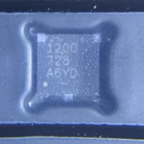
Sink/source DDR termination regulator, DDR/DDR2/DDR3/DDR4 VTT, 3A, VSON-10 (3x3 mm)

10766

有效库存
转到查询

Image for reference only

制造商零件:

TPS51200DRC

包装:

VSON-10(3 x 3 毫米)

品牌:
您可能感兴趣的其他建议.
说明

The TPS51200DRC is a 3A sink/source DDR termination regulator from Texas Instruments in a VSON-10 (3×3 mm) package with exposed thermal pad. It generates the VTT bus termination voltage for DDR, DDR2, DDR3, DDR3L, LPDDR3, and DDR4 memory systems. Key features include VLDOIN range 1.1V-3.5V, ±10 mA buffered REFOUT (VTTREF), remote sensing (VOSNS), droop compensation, PGOOD monitoring, EN-controlled S3 discharge, soft-start, UVLO, OCL, and thermal shutdown. Requires only 20 µF minimum output capacitance (3 x 10 µF MLCCs). Operating range: -40°C to +85°C. Green and Pb-free rated, MSL-2.

The TPS51200DRC is a sink and source Double Data Rate (DDR) termination regulator manufactured by Texas Instruments, specifically designed for low input voltage, low-cost, low-noise systems where space is a key consideration. It maintains a fast transient response and requires a minimum output capacitance of only 20 µF (typically 3 x 10 µF MLCCs), making it one of the most compact and cost-effective VTT regulation solutions available.

The device integrates a high-performance low-dropout (LDO) linear regulator capable of both sourcing and sinking current up to 3 A, making it ideal for DDR memory bus termination applications. The output voltage (VO) tracks the reference input (REFIN) voltage, which can be connected directly to the memory supply voltage (VDDQ) or through a resistor divider, providing flexibility for DDR, DDR2, DDR3, DDR3L, LPDDR3, and DDR4 VTT applications.

Key features include a VLDOIN voltage range of 1.1V to 3.5V supporting both 2.5V and 3.3V power rails, a ±10 mA buffered reference output (REFOUT) for generating the VTTREF reference voltage used by DDR memory controllers, remote voltage sensing (VOSNS) for tight regulation at the load, built-in droop compensation, soft-start current limiting, undervoltage lockout (UVLO), overcurrent protection (OCL), and thermal shutdown.

The TPS51200 provides an open-drain PGOOD signal to monitor output regulation status and an EN (enable) input that can be used to discharge VTT during S3 (suspend-to-RAM) state for DDR power management. The DRC package is a thermally efficient 10-pin VSON (Very thin Small Outline No-lead) with exposed thermal pad, measuring 3.00 x 3.00 mm. The device operates from -40°C to +85°C and is rated both Green and Pb-free.

The TPS51200DRC operates as a bidirectional (sink/source) linear termination voltage regulator, generating the VTT bus termination voltage for DDR memory systems.

Output Voltage Regulation: The output voltage (VO) is regulated to match the reference input (REFIN). For standard DDR termination, REFIN is typically connected to a resistor divider from VDDQ (the memory supply voltage) such that REFIN = VDDQ / 2. The internal error amplifier compares the sensed output voltage (via VOSNS) against the REFIN-derived reference, driving the pass element to source or sink current as needed to maintain VO = VDDQ / 2. This half-VDDQ tracking is the standard VTT voltage required by DDR memory specifications.

Sink and Source Capability: Unlike unidirectional LDO regulators, the TPS51200 can both source current (when VTT load demands more current, e.g., driving DQ lines LOW) and sink current (when VTT load returns current, e.g., driving DQ lines HIGH). This bidirectional capability is essential for DDR termination, where the termination resistors connected to VTT must both absorb and supply current depending on the data bus state. The integrated high-side and low-side pass elements enable this sink/source operation without external components.

Droop Compensation: The device includes built-in droop compensation that pre-adjusts the output voltage slightly higher under heavy sink conditions and slightly lower under heavy source conditions. This anticipatory compensation counteracts the parasitic resistance in PCB traces and vias, maintaining tighter effective regulation at the DDR DIMM termination point.

Reference Output (REFOUT): The REFIN voltage is buffered and output on the REFOUT pin, providing a ±10 mA buffered reference voltage (VTTREF) for DDR memory controllers. REFOUT becomes active when REFIN exceeds 0.390V and VIN is above the UVLO threshold. When REFOUT drops below 0.375V, it is disabled and discharged to GND through an internal 10 kΩ MOSFET. A 0.1 µF ceramic capacitor to GND is required on REFOUT for stability. REFOUT operation is independent of the EN pin state.

Soft-Start Sequencing: At startup, a current clamp implements soft-start by limiting the output current to a low constant value, allowing the output capacitors to charge linearly. This prevents inrush current spikes that could damage the device or cause system voltage rail droops. Once the output reaches the target voltage, the current clamp is released and the regulator enters normal operation.

S3/S5 Power State Support: The EN pin serves dual purpose: when HIGH, the VO regulator is enabled; when LOW (connected to SLP_S3 signal), the VO regulator is disabled and VTT is discharged through an internal MOSFET to GND. This discharge path ensures VTT returns to 0V during suspend-to-RAM (S3) state, meeting DDR power sequencing requirements. REFOUT remains active during S3 state as it is independent of EN.

Power Good (PGOOD): The open-drain PGOOD output goes HIGH-impedance (after a 1 ms deglitch delay) when VO is within ±5% of the target voltage, indicating proper regulation. PGOOD goes LOW (asserted) when VO is out of regulation, during UVLO, during thermal shutdown, or when EN is LOW.

Protection Mechanisms: UVLO disables the device when VIN drops below the threshold (approximately 2.1V), preventing erratic operation during power-up/power-down. Overcurrent protection (OCL) limits the output current to prevent damage during fault conditions. Thermal shutdown disables the device when junction temperature exceeds approximately 150°C, with automatic recovery when temperature drops.

针脚 名称 类型 默认功能 说明
1 REFIN I Reference Input Sets the target output voltage; connect to VDDQ/2 via resistor divider or directly; range 0.5V to 1.8V
2 VLDOIN I LDO Supply Input Power supply for the LDO regulator; range 1.1V to 3.5V; connect to VDDQ or VDD for DDR3/DDR4
3 VO O LDO Output Termination voltage output (VTT); source/sink up to 3A; connect to DDR termination bus
4 PGND G Power Ground Power ground for the LDO; connect to thermal pad and system GND
5 VOSNS I Voltage Sense Input Remote sensing of output voltage; connect to positive terminal of output capacitor or load for tight regulation
6 REFOUT O Reference Output Buffered reference output (VTTREF); ±10 mA drive; requires 0.1 µF ceramic cap to GND; max total cap 0.47 µF
7 EN I Enable Input Enable/disable control; connect to SLP_S3 for DDR VTT control; LOW = VO disabled and discharged
8 接地 G Signal Ground Signal ground reference
9 PGOOD O 电源良好 Open-drain output; HIGH-Z when VO in regulation (±5%); requires external pull-up resistor
10 VIN I 电源 2.5V or 3.3V main power supply; requires 1 µF to 4.7 µF ceramic decoupling capacitor
垫子 隔热垫 G Thermal/PGND Exposed thermal pad; connect to PGND and system GND plane for heat dissipation
应用 说明
DDR3/DDR4 VTT Termination Primary application: generating and regulating VTT bus termination voltage for DDR3 (0.75V), DDR3L (0.675V), LPDDR3 (0.6V), and DDR4 (0.6V) memory systems in notebooks, desktops, and servers
DDR2 VTT Termination Generating 0.9V VTT for DDR2 memory systems with 1.8V VDDQ; REFIN set to VDDQ/2 via resistor divider
Embedded DDR Memory VTT regulation for embedded systems, SoC boards, and compute modules using DDR3/DDR4 with minimal external components
Telecom and Networking VTT supply for DDR memory in routers, switches, base stations, and telecom equipment; supports S3 power state for energy savings
General-Purpose LDO Can be used as a general-purpose sink/source LDO for applications requiring bidirectional current capability and tight tracking regulation
模型 制造商 兼容性 主要区别
TPS51200A TI Pin-Compatible / Drop-in Upgrade Enhanced robustness version; same package and function; recommended for new designs
TPS51200DRCR TI Pin-Compatible / Identical Large tape and reel packaging (3,000/reel) vs small reel (250/reel); same silicon
TPS51100 TI 功能相似 Earlier generation; higher VIN min (4.75V); MSOP-10 PowerPAD package; not suitable for 2.5V rail
TPS51200-Q1 TI 针脚兼容 Automotive qualified (AEC-Q100); -40°C to +125°C; same functionality with automotive grade
NCP51399 onsemi 功能相似 DDR3/DDR4 termination regulator; 3A sink/source; DFN-10 package; different pinout
推荐部件
PMIC for AM335x, 3 DC-DC, 4 LDO, Li-ion charger, WLED driver, VQFN-48

品牌:

封装:

VQFN-48 (6 x 6 x 0.9 mm, 0.4 mm pitch, with thermal pad)
有库存:
4012pcs

货运周期:3~7 天
最低订购量为 1

转到查询
Octal D-type flip-flop with clear, 2-6V, 28 MHz, SOP-20

品牌:

封装:

SOP-20 NS (10.2 x 5.3 mm)
有库存:
7821pcs

货运周期:3~7 天
最低订购量为 1

转到查询
3-to-8 line decoder/demux, active-low outputs, 2-6V, PDIP-16

品牌:

封装:

PDIP-16 (19.3 x 6.35 mm)
有库存:
10248pcs

货运周期:3~7 天
最低订购量为 1

转到查询
2W mono Class-AB audio amp, BTL/SE, 2.5-5.5V, HVSSOP-8 PowerPAD

品牌:

封装:

HVSSOP-8 (DGN) with PowerPAD (4.9 x 3.9 mm)
有库存:
9105pcs

货运周期:3~7 天
最低订购量为 1

转到查询
10/100 Ethernet PHY transceiver, MII/RMII/SNI, 3.3V, LQFP-48, commercial temp

品牌:

封装:

LQFP-48 (7 x 7 mm)
有库存:
5472pcs

货运周期:3~7 天
最低订购量为 1

转到查询
Octal bus transceiver, 3-state outputs, 2-6V, 8-channel, TSSOP-20

品牌:

封装:

TSSOP-20 (6.5 x 4.4 mm)
有库存:
7654pcs

货运周期:3~7 天
最低订购量为 1

转到查询
质量保证

我们从合作供应链采购的所有电子元件都经过严格的进货检验。通过仔细的测试,我们确保交付给客户的所有产品都是原装正品,符合质量要求。此外,我们还保存完整的检验记录,使整个供应链流程清晰可查。.

认证
我们获得了多项专业认证,并建立了自己的专业检测实验室,确保交付给客户的每一件产品都符合最高质量要求。我们严格按照流程进行检测,确保产品质量稳定、参数准确。为保证原装正品,我们还与可靠的第三方检测机构合作,进行严格的质量检测。我们始终高度重视质量,完全符合行业标准、相关法规和 ISO 9001:2015 的要求。.

发货与付款

我们从合作供应链采购的所有电子元件都经过严格的进货检验。通过仔细的测试,我们确保交付给客户的所有产品都是原装正品,符合质量要求。此外,我们还保存完整的检验记录,使整个供应链流程清晰可查。.

认证
我们获得了多项专业认证,并建立了自己的专业检测实验室,确保交付给客户的每一件产品都符合最高质量要求。我们严格按照流程进行检测,确保产品质量稳定、参数准确。为保证原装正品,我们还与可靠的第三方检测机构合作,进行严格的质量检测。我们始终高度重视质量,完全符合行业标准、相关法规和 ISO 9001:2015 的要求。.

服务与包装

我们从合作供应链采购的所有电子元件都经过严格的进货检验。通过仔细的测试,我们确保交付给客户的所有产品都是原装正品,符合质量要求。此外,我们还保存完整的检验记录,使整个供应链流程清晰可查。.

认证
我们获得了多项专业认证,并建立了自己的专业检测实验室,确保交付给客户的每一件产品都符合最高质量要求。我们严格按照流程进行检测,确保产品质量稳定、参数准确。为保证原装正品,我们还与可靠的第三方检测机构合作,进行严格的质量检测。我们始终高度重视质量,完全符合行业标准、相关法规和 ISO 9001:2015 的要求。.



