首页 > 集成电路 IC > STM32F103RBT6

STM32F103RBT6


ARM Cortex-M3、72MHz、128KB 闪存、20KB SRAM、2xADC 12 位、3xUSART、2xSPI、2xI2C、USB FS、CAN、LQFP-64、51 I/O、2.0-3.6V、-40~85C

15000

有效库存
转到查询

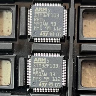
Image for reference only

制造商零件:

STM32F103RBT6

包装:

LQFP-64(10 x 10 x 1.4 毫米,0.5 毫米间距)

品牌:
产品类别:
您可能感兴趣的其他建议.
说明

The STM32F103RBT6 from STMicroelectronics is a mainstream performance line ARM Cortex-M3 32-bit RISC microcontroller operating at up to 72 MHz in a 64-pin LQFP package (10 x 10 x 1.4 mm). Key specifications: 128 Kbytes Flash memory; 20 Kbytes SRAM; 51 programmable I/O pins (most 5V tolerant). Two 12-bit ADCs with up to 16 external channels (1 us conversion time), dual sample-and-hold, and internal temperature sensor. Seven timers: three 16-bit general-purpose timers with up to 4 IC/OC/PWM channels and quadrature encoder input; one 16-bit motor control PWM timer with dead-time generation and emergency stop; two watchdog timers (independent and window); one 24-bit SysTick downcounter. Nine communication interfaces: up to two I2C (SMBus/PMBus, 400 kHz); up to three USARTs (ISO 7816, LIN, IrDA, modem control); up to two SPI (18 Mbit/s); one USB 2.0 full-speed device with on-chip PHY; one CAN 2.0B Active. 7-channel DMA controller supporting timers, ADC, SPI, I2C, and USART. Clock management: 4-16 MHz external crystal, internal 8 MHz RC (trimmed), internal 40 kHz RC, 32 kHz RTC oscillator with calibration, PLL for CPU clock. Power: 2.0-3.6V; low-power modes (Sleep, Stop, Standby); VBAT for RTC and backup registers. Debug: SWD and JTAG. CRC calculation unit. 96-bit unique ID. Operating temperature -40C to +85C. ECOPACK2, ECCN 3A991.a.2. Active product.

The STM32F103RBT6 from STMicroelectronics is a mainstream performance line ARM Cortex-M3 microcontroller that offers an excellent balance of processing power, peripheral integration, and cost-effectiveness in a 64-pin LQFP package. With 128 KB of Flash memory and 20 KB of SRAM, it provides sufficient resources for a wide range of embedded applications, from motor control to industrial communication.

The STM32F103RBT6 is part of the medium-density STM32F103xx family, which includes devices with 64 or 128 KB Flash in packages from 36 to 100 pins. The R suffix denotes a 64-pin package, the B suffix denotes 128 KB Flash, and the T6 suffix denotes LQFP package with -40C to +85C industrial temperature range. This positions the STM32F103RBT6 as a step up from the popular STM32F103C8T6 (48-pin LQFP, 64 KB Flash), offering more GPIO (51 vs 37), more Flash (128 KB vs 64 KB), and the addition of CAN and USB interfaces.

The ARM Cortex-M3 core delivers 1.25 DMIPS/MHz at 72 MHz, providing 90 DMIPS of processing power. While significantly less powerful than the Cortex-M4-based STM32F4 series (168 MHz, FPU, DSP), the Cortex-M3 is more than adequate for real-time control, communication protocol processing, and moderate computational workloads. The lack of a hardware FPU means floating-point operations are emulated in software, which is acceptable for many control applications but may be a bottleneck for heavy signal processing.

The dual 12-bit ADCs are a key strength, providing up to 16 external channels with 1 us conversion time. In dual ADC mode, the two ADCs can operate simultaneously, enabling synchronized sampling of multiple channels (e.g., sampling all three phases of a motor simultaneously). The internal temperature sensor provides die temperature monitoring for thermal management. The ADC supports DMA transfers, enabling continuous conversion without CPU intervention.

The motor control PWM timer (TIM1) provides six PWM channels with complementary output, dead-time insertion, and break input for emergency stop. This makes the STM32F103RBT6 suitable for 3-phase motor control applications including BLDC, PMSM, and AC induction motor drives. The quadrature encoder interface in the general-purpose timers simplifies connection to incremental encoders for position feedback.

The USB 2.0 full-speed device interface includes an on-chip PHY, requiring only an external 1.5 kOhm pull-up resistor on the DP line. The USB peripheral supports all standard USB device classes (CDC, HID, MSC, custom) and includes dedicated USB SRAM buffers. The CAN 2.0B interface supports both standard (11-bit) and extended (29-bit) identifiers with three transmit mailboxes, two receive FIFOs, and loop-back/silent modes for diagnostics.

The 7-channel DMA controller offloads data transfer tasks from the CPU, enabling high-throughput communication (SPI, I2C, USART), continuous ADC sampling, and memory-to-memory transfers without CPU intervention. Each DMA channel can be configured for peripheral-to-memory, memory-to-peripheral, or memory-to-memory transfers with configurable priority levels.

The LQFP-64 package exposes 51 of the possible 80 GPIO pins, providing a good balance between I/O availability and board space. The exposed pins include all of Port A (16 pins), Port B (16 pins), most of Port C (13 pins), and a few Port D pins. This is sufficient for most medium-complexity applications while keeping the PCB layout manageable.

The STM32F103RBT6 operates as a 32-bit ARM Cortex-M3 microcontroller with on-chip Flash, SRAM, and an extensive peripheral set connected through a multi-bus matrix.

ARM Cortex-M3 Core: The Cortex-M3 implements the ARMv7-M architecture with a 3-stage pipeline (fetch, decode, execute). It supports 56 base instructions plus additional DSP extensions including saturated arithmetic, multiply-accumulate (MAC), and hardware divide. The NVIC (Nested Vectored Interrupt Controller) supports up to 43 maskable interrupt channels plus the non-maskable interrupt (NMI), with 16 programmable priority levels. The interrupt latency is deterministic at 12 cycles (6 cycles tail-chaining). The processor includes a Memory Protection Unit (MPU) with 8 regions for privilege separation and memory access control.

Bus Matrix: The multi-AHB bus matrix connects the Cortex-M3 core, DMA controller, and peripherals through three AHB buses: I-bus (instruction fetch from Flash/SRAM), D-bus (data access from Flash/SRAM), and S-bus (system bus for peripheral register access). The DMA controller shares access to SRAM and peripherals through the bus matrix, enabling concurrent CPU and DMA operations when they access different targets. The AHB is clocked at up to 72 MHz, with the APB1 bus at up to 36 MHz and the APB2 bus at up to 72 MHz.

Flash Memory with Prefetch: The Flash memory has a native access time that requires wait states at 72 MHz (typically 2 wait states). The prefetch buffer (2 x 64-bit lines) fetches the next instruction ahead of the current execution, mitigating the wait-state penalty for linear code execution. Branches and random accesses still incur the full wait-state penalty.

Clock System: The clock tree provides flexible clock configuration. The System Clock (SYSCLK) can be sourced from HSI (8 MHz internal RC), HSE (4-16 MHz external crystal), or PLL. The PLL can multiply the HSE or HSE/2 to generate up to 72 MHz. The AHB prescaler divides SYSCLK for the AHB bus, and the APB1/APB2 prescalers further divide the AHB clock for the peripheral buses. The RTC can use LSE (32.768 kHz crystal) or LSI (40 kHz internal RC) for independent timekeeping.

ADC Dual Mode: The two ADCs can operate independently or in combined modes. In regular simultaneous mode, both ADCs convert different channels at the same time. In fast interleaved mode, both ADCs alternate conversions on the same channel to double the sampling rate. In slow interleaved mode, ADC1 and ADC2 alternate conversions with a delay for higher precision. The dual sample-and-hold circuits allow simultaneous sampling of two channels, which is essential for power metering and motor control where phase relationships must be preserved.

Motor Control Timer: TIM1 is an advanced-control timer specifically designed for motor drive applications. It provides up to 6 PWM outputs arranged as 3 complementary pairs (CH1/CH1N, CH2/CH2N, CH3/CH3N), with programmable dead-time insertion between complementary outputs to prevent shoot-through in half-bridge configurations. The break input (BKIN) provides emergency shutdown capability, immediately forcing all PWM outputs to a safe state. The repetition counter reduces the update event rate for slower control loops.

DMA Controller: The 7-channel DMA1 controller supports circular mode for continuous data acquisition (e.g., ADC samples streaming to SRAM), and normal mode for one-shot transfers. Each channel has configurable source and destination addresses, transfer width (byte/half-word/word), and transfer count. Interrupts on transfer complete, half-transfer, and transfer error allow the CPU to process data without polling.

Pin Range 名称 类型 说明
1 VBAT 电源 Battery backup supply for RTC, backup registers, and backup SRAM; connect to VDD or a battery/supercap; maintains time and data when main power is removed; current consumption in backup mode approximately 1 uA
2 PC13-TAMPER-RTC 输入/输出 Port C bit 13; alternate: Tamper detection input for backup domain, RTC output (alarm, calibration); not 5V tolerant; maximum output speed 2 MHz; primarily used for RTC functions rather than general I/O
3-4 PC14-OSC32_IN / PC15-OSC32_OUT 输入/输出 Port C bits 14-15; alternate: 32.768 kHz low-speed external crystal (LSE) oscillator pins; when LSE is not used, these pins can be GPIO but with limited output speed (2 MHz); not 5V tolerant
5-6 PD0-OSC_IN / PD1-OSC_OUT I/O (FT) Port D bits 0-1; default function after reset: 4-16 MHz high-speed external crystal (HSE) oscillator pins; when HSE is not used, PD0/PD1 can be remapped as general-purpose I/O via AFIO; 5V tolerant; PD0 also serves as FSMC_D2 in 100-pin devices
7 NRST I/O (Reset) Active-low reset input with built-in pull-up; a low pulse longer than the minimum width generates a system reset; connect 10k pull-up to VDD and 100nF cap to VSS for noise filtering; optional reset button to GND; reset also generated internally by POR, PDR, WWDG, IWDG, and SWD command
8 PC0-PC5 I/O (FT) Port C bits 0-5; alternate: ADC1/2 channels 10-15 (12-bit); also TIM3/4 capture/compare, I2C2, SPI2 in remapped configurations; all 5V tolerant; commonly used for analog sensor inputs due to ADC availability
9-16 PA0-PA7 I/O (FT) Port A bits 0-7; PA0=WKUP/ADC1_IN0/TIM2_CH2/TIM5_CH1; PA1=ADC1_IN1/TIM5_CH2; PA2=ADC1_IN2/USART2_TX; PA3=ADC1_IN3/USART2_RX; PA4=ADC1_IN4/SPI1_NSS; PA5=ADC1_IN5/SPI1_SCK; PA6=ADC1_IN6/SPI1_MISO/TIM3_CH1; PA7=ADC1_IN7/SPI1_MOSI/TIM3_CH2; all 5V tolerant
17-24 PA8-PA15 I/O (FT) Port A bits 8-15; PA8=MCO/TIM1_CH1; PA9=USART1_TX/TIM1_CH2; PA10=USART1_RX/TIM1_CH3; PA11=USBDM/CAN_RX/TIM1_CH4; PA12=USBDP/CAN_TX/TIM1_ETR; PA13=SWDIO/JTMS; PA14=SWCLK/JTCK; PA15=JTDI/SPI1_NSS(remap); PA13/PA14 are debug pins by default
25-32 PB0-PB7 I/O (FT) Port B bits 0-7; PB0=ADC1_IN8/TIM3_CH3/TIM1_CH2N; PB1=ADC1_IN9/TIM3_CH4/TIM1_CH3N; PB2=BOOT1; PB3=JTDO/TIM2_CH2/SPI1_SCK(remap); PB4=NJTRST/TIM3_CH1/SPI1_MISO(remap); PB5=I2C1_SMBA/TIM3_CH2/SPI1_MOSI(remap); PB6=I2C1_SCL/TIM4_CH1/USART1_TX(remap); PB7=I2C1_SDA/TIM4_CH2/USART1_RX(remap)
33-40 PB8-PB15 I/O (FT) Port B bits 8-15; PB8=TIM4_CH3/CAN_RX/I2C1_SCL(remap)/SDIO_D4; PB9=TIM4_CH4/CAN_TX/I2C1_SDA(remap)/SDIO_D5; PB10=I2C2_SCL/USART3_TX; PB11=I2C2_SDA/USART3_RX; PB12=SPI2_NSS/I2C2_SMBA/USART3_CK/TIM1_BKIN; PB13=SPI2_SCK/USART3_CTS/TIM1_CH1N; PB14=SPI2_MISO/USART3_RTS/TIM1_CH2N; PB15=SPI2_MOSI/TIM1_CH3N
41 PC6-PC12 I/O (FT) Port C bits 6-12; alternate: TIM3/4/8 channels, USART3/6, I2C, SDIO, TIM5 (remap); commonly used for timer PWM and USART communication
42 PC13/PC14/PC15 输入/输出 See pins 2-4 above; limited GPIO capability; not 5V tolerant
43 PD2 I/O (FT) Port D bit 2; alternate: USART3_RTS/TIM3_ETR/SDIO_CMD; 5V tolerant; one of the few Port D pins exposed in LQFP-64
44 BOOT0 输入 Boot mode selection pin; LOW = boot from Main Flash (normal operation); HIGH = boot from System Memory (built-in bootloader for UART/USB/SWD programming); connect with 10k pull-down to GND; add jumper or switch to VDD for ISP programming mode; do not leave floating
应用 说明
3-Phase Motor Drive Use TIM1 motor control PWM timer for 6-channel complementary PWM with dead-time generation; dual ADC for simultaneous 3-phase current sampling; quadrature encoder interface on TIM3/4 for position feedback; CAN bus for drive communication; 128KB Flash stores FOC algorithm, communication stack, and protection logic; 20KB SRAM buffers ADC data and control variables; 72MHz provides sufficient headroom for 10-20kHz control loop
USB-CAN Gateway Bridge between USB and CAN networks; USB FS device for PC connection; CAN 2.0B for industrial bus; 128KB Flash stores USB and CAN protocol stacks plus application code; DMA offloads data transfer between USB and CAN buffers; dual ADC for monitoring bus voltages; multiple USARTs for debug and auxiliary communication
Industrial Data Acquisition 16-channel 12-bit ADC with dual simultaneous sampling for synchronized multi-sensor acquisition; DMA streams ADC data to SRAM without CPU overhead; 7-channel DMA handles concurrent ADC, SPI, and USART transfers; TIM1/2/3 generate precise timing for sample-and-hold circuits; I2C for digital sensors; SPI for external ADC expansion; 128KB Flash stores acquisition parameters and data processing algorithms
Smart Meter / Power Monitor Dual ADC simultaneously samples voltage and current waveforms for power calculation; 72MHz Cortex-M3 computes RMS, power factor, and harmonics in real time; 20KB SRAM buffers waveform data; USART for Modbus RTU communication; CAN for fieldbus integration; RTC with backup battery for time-stamping; 128KB Flash stores metering firmware and calibration tables
Embedded Web Server (with external MAC) Use SPI to connect external Ethernet controller (e.g., W5100, ENC28J60); 128KB Flash stores HTTP server, TCP/IP stack, and application logic; 20KB SRAM for network buffers; USART for debug console; USB for configuration interface; multiple timers for scheduling and watchdog; 51 GPIO pins for control outputs and status inputs
模型 制造商 兼容性 主要区别
STM32F103R8T6 ST Same Package, Less Flash Same LQFP-64 pinout and peripherals; 64KB Flash instead of 128KB; same 20KB SRAM; same USB, CAN, ADC, timers; use when 64KB Flash is sufficient; lower cost; drop-in replacement with reduced program space
STM32F103C8T6 ST Smaller Package LQFP-48 (7x7mm) vs LQFP-64; 64KB Flash (originally, now generally 128KB in production); 37 I/O vs 51; same Cortex-M3 at 72MHz; same peripherals but fewer exposed pins; no CAN or USB in all pin configurations; the most popular and lowest-cost STM32F1 variant; use for cost-sensitive designs with fewer I/O requirements
STM32F103VET6 ST Larger Package, More Features LQFP-100 (14x14mm); 512KB Flash, 64KB SRAM; 80 I/O; adds FSMC for external memory, more timers, DAC; more GPIO ports (D, E); use when more memory, more I/O, or FSMC is needed; higher cost but much more capability
STM32F401RBT6 ST Same Package, Newer Core Same LQFP-64 footprint; Cortex-M4 with FPU at 84MHz; 128KB Flash, 64KB SRAM; no CAN or Ethernet; USB FS; higher performance CPU with floating-point hardware; use for new designs needing FPU without changing PCB layout
LPC1758FBD80 恩智浦 竞争性替代方案 Cortex-M3 at 100MHz; 512KB Flash, 64KB SRAM; LQFP-80; Ethernet MAC, USB, CAN, I2S; higher clock speed and more memory; different tool chain and peripheral register set; use as ARM Cortex-M3 alternative with more headroom
推荐部件
Cortex-M7 MCU, 216 MHz, 2MB Flash, 512KB SRAM, LQFP-144, DPFPU, Chrom-ART

品牌:

封装:

LQFP-144 (20 x 20 x 1.4 mm)
有库存:
1935pcs

货运周期:3~7 天
最低订购量为 1

转到查询
Ultra-low-power Cortex-M0+ MCU, 32 MHz, 128KB Flash, USB, LQFP-64

品牌:

封装:

LQFP-64(10 x 10 x 1.4 毫米)
有库存:
6745pcs

货运周期:3~7 天
最低订购量为 1

转到查询
Arm Cortex-M4 MCU, 168 MHz, 512KB Flash, 192KB SRAM, Ethernet, USB OTG, LQFP-100

品牌:

封装:

LQFP-100 (14 x 14 x 1.4 mm)
有库存:
11237pcs

货运周期:3~7 天
最低订购量为 1

转到查询
ARM Cortex-M4F MCU, 72MHz, 384KB Flash, 64KB SRAM, dual ADC, 4 comparators, 2 op amps, LQFP-100

品牌:

封装:

LQFP-100 (14 x 14 x 1.4 mm)
有库存:
12274pcs

货运周期:3~7 天
最低订购量为 1

转到查询
ARM Cortex-M4F MCU, 168MHz, 1MB Flash, 192KB SRAM, Ethernet, USB OTG HS, UFBGA-176

品牌:

封装:

UFBGA-176 (10 x 10 mm, 0.65mm pitch)
有库存:
9303pcs

货运周期:3~7 天
最低订购量为 1

转到查询
Quad JFET-input op amp, 4MHz GBP, 16V/µs slew rate, 200pA bias current, SOIC-14

品牌:

封装:

SOIC-14 (8.75 x 4 x 1.65 mm)
有库存:
9834pcs

货运周期:3~7 天
最低订购量为 1

转到查询
质量保证

我们从合作供应链采购的所有电子元件都经过严格的进货检验。通过仔细的测试,我们确保交付给客户的所有产品都是原装正品,符合质量要求。此外,我们还保存完整的检验记录,使整个供应链流程清晰可查。.

认证
我们获得了多项专业认证,并建立了自己的专业检测实验室,确保交付给客户的每一件产品都符合最高质量要求。我们严格按照流程进行检测,确保产品质量稳定、参数准确。为保证原装正品,我们还与可靠的第三方检测机构合作,进行严格的质量检测。我们始终高度重视质量,完全符合行业标准、相关法规和 ISO 9001:2015 的要求。.

发货与付款

我们从合作供应链采购的所有电子元件都经过严格的进货检验。通过仔细的测试,我们确保交付给客户的所有产品都是原装正品,符合质量要求。此外,我们还保存完整的检验记录,使整个供应链流程清晰可查。.

认证
我们获得了多项专业认证,并建立了自己的专业检测实验室,确保交付给客户的每一件产品都符合最高质量要求。我们严格按照流程进行检测,确保产品质量稳定、参数准确。为保证原装正品,我们还与可靠的第三方检测机构合作,进行严格的质量检测。我们始终高度重视质量,完全符合行业标准、相关法规和 ISO 9001:2015 的要求。.

服务与包装

我们从合作供应链采购的所有电子元件都经过严格的进货检验。通过仔细的测试,我们确保交付给客户的所有产品都是原装正品,符合质量要求。此外,我们还保存完整的检验记录,使整个供应链流程清晰可查。.

认证
我们获得了多项专业认证,并建立了自己的专业检测实验室,确保交付给客户的每一件产品都符合最高质量要求。我们严格按照流程进行检测,确保产品质量稳定、参数准确。为保证原装正品,我们还与可靠的第三方检测机构合作,进行严格的质量检测。我们始终高度重视质量,完全符合行业标准、相关法规和 ISO 9001:2015 的要求。.



