首页 > 集成电路 IC > SN74LVC138APWR

SN74LVC138APWR


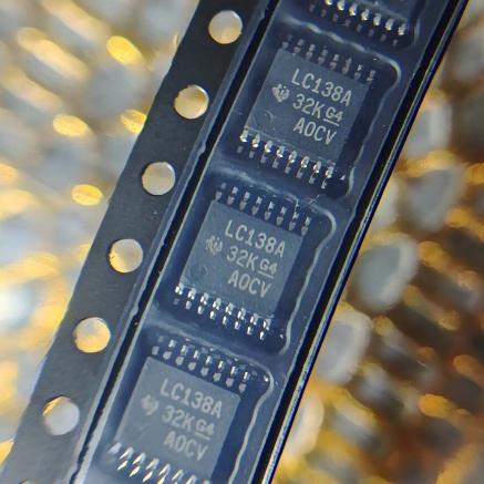
3-to-8 line decoder/demultiplexer, 1.65-3.6V, 5V-tolerant inputs, 5.8ns tpd, TSSOP-16, -40~85C

15876

有效库存
转到查询

Image for reference only

制造商零件:

SN74LVC138APWR

包装:

TSSOP-16 (PW) (5.0 x 4.4 x 1.05 mm)

品牌:
产品类别:
您可能感兴趣的其他建议.
说明

The SN74LVC138APWR from Texas Instruments is a 3-line to 8-line decoder/demultiplexer in a 16-pin TSSOP package, designed for high-performance memory decoding and data routing applications. The device features three binary-weighted address inputs (A0, A1, A2) that select one of eight active-low outputs (Y0-Y7). Three enable inputs (two active-low G2A, G2B and one active-high G1) provide flexible cascading for expansion to 24-line or 32-line decoders without external inverters. Operating voltage: 1.65V to 3.6V, with 5V-tolerant inputs for mixed-voltage systems. Maximum propagation delay: 5.8ns at 3.3V. Output drive: plus/minus 24mA. Quiescent current: 10uA max. Latch-up exceeds 250mA per JESD 17. -40C to 85C. MSL-1, RoHS, EAR99. Tape and reel, 2000/reel.

The SN74LVC138APWR from Texas Instruments is a 3-line to 8-line decoder/demultiplexer housed in a 16-pin TSSOP package, designed for high-performance memory decoding and data routing applications requiring very short propagation delay times.

The device features three binary-weighted address inputs (A0, A1, A2) that select one of eight mutually exclusive active-low outputs (Y0 through Y7). Three enable inputs provide flexible control: two active-low enables (G2A, G2B) and one active-high enable (G1). The decoder is enabled only when G1 is HIGH and both G2A and G2B are LOW. When disabled, all outputs are forced HIGH regardless of the address inputs.

The multiple enable inputs facilitate easy cascading for address expansion. Four SN74LVC138A devices plus one inverter can implement a 1-of-32 (5-to-32 line) decoder without additional logic. A single enable input can also serve as a data input for demultiplexing applications, distributing a single data stream to one of eight output lines.

Key specifications include: supply voltage 1.65V to 3.6V (single supply), 5.5V-tolerant inputs enabling use as a 3.3V-to-5V logic translator, maximum propagation delay of 5.8ns at 3.3V, output drive current of plus/minus 24mA, maximum quiescent current of 10uA, and latch-up performance exceeding 250mA per JESD 17. The typical output ground bounce is less than 0.8V and output VOH undershoot exceeds 2V at VCC=3.3V.

The LVC (Low-Voltage CMOS) technology provides the optimal combination of high speed, low power, and wide voltage compatibility. The 74LVC138A is functionally identical to the industry-standard 74LS138 and 74HC138 but with broader voltage range and 5V-tolerant inputs. The PW suffix denotes TSSOP-16 package, R suffix denotes tape and reel with 2,000 units per reel. The device is RoHS compliant, MSL Level 1, EAR99 classified.

The SN74LVC138APWR operates as a combinational logic decoder that converts a 3-bit binary address into one-of-eight active-low output selections, with enable inputs for cascading and demultiplexing.

Decoding Logic: The three address inputs A0 (LSB), A1, and A2 (MSB) form a 3-bit binary number from 0 to 7. Internally, the device implements eight 3-input AND gates, each fed by a unique combination of the address inputs (or their complements). For address value N, the corresponding output YN is driven LOW while all other outputs remain HIGH. Since all outputs are active-low, the selected output is the one that goes LOW. For example, if A2=0, A1=1, A0=0 (binary 010 = decimal 2), output Y2 goes LOW while Y0, Y1, Y3-Y7 remain HIGH.

Enable Logic: The three enable inputs (G1, G2A, G2B) gate all eight output AND gates. The decoder is enabled only when G1=HIGH AND G2A=LOW AND G2B=LOW. If any enable condition is not met, all eight outputs are forced HIGH regardless of the address inputs. The enable logic expression is: Enable = G1 AND (NOT G2A) AND (NOT G2B). The dual active-low enables (G2A, G2B) are particularly useful for cascading: one can serve as a chip select from higher-order address lines while the other provides system-level enable/disable control.

Cascading for Address Expansion: To build a 1-of-16 decoder, two SN74LVC138A devices are used. The most significant address bit (A3) connects to the enable inputs: one decoder is enabled when A3=0 (via G2A), and the other when A3=1 (via G1). For a 1-of-32 decoder, four devices are cascaded using a fifth address bit (A4) to select one of four decoder enable combinations. Two active-low enables and one active-high enable provide maximum flexibility in cascading configurations without requiring external inverters.

Demultiplexing Mode: When used as a demultiplexer, one of the enable inputs serves as the data input. For example, connecting the serial data stream to G1 while keeping G2A=G2B=LOW routes the data to the output selected by the current address. When the data input is HIGH, the selected output goes LOW (active); when LOW, all outputs go HIGH. This provides 1-to-8 data distribution under address control.

5V-Tolerant Inputs: The LVC family inputs can accept voltages up to 5.5V regardless of the VCC supply level. This enables the device to translate between 3.3V and 5V logic systems: a 5V microcontroller can drive the address and enable inputs of a 3.3V-supplied SN74LVC138A without level shifters. The output levels are determined by VCC, so the decoded outputs will be 3.3V logic levels.

针脚 名称 类型 说明
1 A0 输入 Address input LSB; 5.5V tolerant; selects output line Y0-Y7 based on 3-bit binary value
2 A1 输入 Address input middle bit; 5.5V tolerant; combines with A0 and A2 to select active output
3 A2 输入 Address input MSB; 5.5V tolerant; determines which group of four outputs (Y0-3 or Y4-7) is active
4 /G2A 输入 Active-low enable input; decoder active only when G2A=LOW, G2B=LOW, and G1=HIGH simultaneously
5 /G2B 输入 Active-low enable input; can serve as chip select or data input for demultiplexing; 5.5V tolerant
6 G1 输入 Active-high enable input; decoder enabled when HIGH with both G2A and G2B LOW; 5.5V tolerant
7 /Y7 输出 Active-low decoded output 7; selected when A2A1A0 = 111; sinks up to 24mA
8 接地 电源 接地;连接至系统地平面
9 /Y6 输出 Active-low decoded output 6; selected when A2A1A0 = 110
10 /Y5 输出 Active-low decoded output 5; selected when A2A1A0 = 101
11 /Y4 输出 Active-low decoded output 4; selected when A2A1A0 = 100
12 /Y3 输出 Active-low decoded output 3; selected when A2A1A0 = 011
13 /Y2 输出 Active-low decoded output 2; selected when A2A1A0 = 010
14 /Y1 输出 Active-low decoded output 1; selected when A2A1A0 = 001
15 /Y0 输出 Active-low decoded output 0; selected when A2A1A0 = 000
16 VCC 电源 Supply voltage; 1.65V to 3.6V; bypass with 0.1uF ceramic capacitor to GND
应用 说明
Memory Address Decoding Decodes upper address bits to generate chip select signals for multiple memory devices; 5.8ns propagation delay ensures zero wait-state operation with fast memories
输入/输出端口扩展 Expands 3 microcontroller GPIO lines into 8 active-low chip select or enable lines; enables individual access to multiple peripheral ICs from limited MCU pins
Data Demultiplexing Distributes a single data stream to one of eight output lines under address control; useful for time-division multiplexed signal routing
Address Expansion Cascading Multiple SN74LVC138A devices cascade to build 1-of-16, 1-of-24, or 1-of-32 decoders; dual active-low and single active-high enables eliminate external logic
Mixed-Voltage Logic Translation 5V-tolerant inputs allow 5V logic to drive 3.3V-supplied decoder; translates 5V address bus to 3.3V output levels without level shifters
模型 制造商 兼容性 主要区别
74HC138PW Nexperia 针脚兼容 HC family (2-6V supply); same logic function; no 5V-tolerant input feature needed since supply can be 5V; different speed/voltage tradeoff
74HCT138PW Nexperia 针脚兼容 HCT family; 4.5-5.5V supply; TTL-compatible input thresholds; ideal for 5V systems interfacing with TTL logic
SN74LVC1G138 TI 功能等同 Single-gate version in tiny SOT-23-6 or VSSOP-8; same 3-to-8 decode; for space-constrained designs with fewer enable options
74AHC138 瑞萨 针脚兼容 AHC family; 2-5.5V supply; faster than HC at 3.3V; intermediate between HC and LVC performance
SN74LVC139APWR TI 功能相似 Dual 2-to-4 decoder in same TSSOP-16; two independent decoders instead of one 3-to-8; different application scope
推荐部件
PMIC for AM335x, 3 bucks, 2 LDOs, battery charger, WLED, I2C, VQFN-48

品牌:

封装:

VQFN-48 (6×6 mm, 0.4 mm pitch)
有库存:
8909pcs

货运周期:3~7 天
最低订购量为 1

转到查询
Octal D-type flip-flop, edge-triggered, async clear, 28MHz, SOP-20

品牌:

封装:

SOP-20 (NS) (12.6×7.8 mm)
有库存:
8359pcs

货运周期:3~7 天
最低订购量为 1

转到查询
3-to-8 decoder/demux, active-low outputs, 3 enable inputs, 15ns, PDIP-16

品牌:

封装:

PDIP-16 (24.33×9.4 mm, Through-Hole)
有库存:
11952pcs

货运周期:3~7 天
最低订购量为 1

转到查询
2W mono Class-AB audio amp, BTL speaker + SE headphone, 2.5-5.5V, HVSSOP-8

品牌:

封装:

HVSSOP-8 (DGN) (3.0×4.9 mm, PowerPAD)
有库存:
3337pcs

货运周期:3~7 天
最低订购量为 1

转到查询
10/100 Ethernet PHY, MII/RMII/SNI, Auto-MDIX, 270mW, LQFP-48, commercial

品牌:

封装:

LQFP-48 (7×7 mm)
有库存:
14754pcs

货运周期:3~7 天
最低订购量为 1

转到查询
Octal bus transceiver, 3-state outputs, 2-6V, 12ns tpd, TSSOP-20

品牌:

封装:

TSSOP-20 (6.5×6.4 mm)
有库存:
2638pcs

货运周期:3~7 天
最低订购量为 1

转到查询
质量保证

我们从合作供应链采购的所有电子元件都经过严格的进货检验。通过仔细的测试,我们确保交付给客户的所有产品都是原装正品,符合质量要求。此外,我们还保存完整的检验记录,使整个供应链流程清晰可查。.

认证
我们获得了多项专业认证,并建立了自己的专业检测实验室,确保交付给客户的每一件产品都符合最高质量要求。我们严格按照流程进行检测,确保产品质量稳定、参数准确。为保证原装正品,我们还与可靠的第三方检测机构合作,进行严格的质量检测。我们始终高度重视质量,完全符合行业标准、相关法规和 ISO 9001:2015 的要求。.

发货与付款

我们从合作供应链采购的所有电子元件都经过严格的进货检验。通过仔细的测试,我们确保交付给客户的所有产品都是原装正品,符合质量要求。此外,我们还保存完整的检验记录,使整个供应链流程清晰可查。.

认证
我们获得了多项专业认证,并建立了自己的专业检测实验室,确保交付给客户的每一件产品都符合最高质量要求。我们严格按照流程进行检测,确保产品质量稳定、参数准确。为保证原装正品,我们还与可靠的第三方检测机构合作,进行严格的质量检测。我们始终高度重视质量,完全符合行业标准、相关法规和 ISO 9001:2015 的要求。.

服务与包装

我们从合作供应链采购的所有电子元件都经过严格的进货检验。通过仔细的测试,我们确保交付给客户的所有产品都是原装正品,符合质量要求。此外,我们还保存完整的检验记录,使整个供应链流程清晰可查。.

认证
我们获得了多项专业认证,并建立了自己的专业检测实验室,确保交付给客户的每一件产品都符合最高质量要求。我们严格按照流程进行检测,确保产品质量稳定、参数准确。为保证原装正品,我们还与可靠的第三方检测机构合作,进行严格的质量检测。我们始终高度重视质量,完全符合行业标准、相关法规和 ISO 9001:2015 的要求。.



