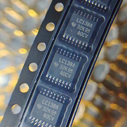
The SN74LVC138APWR operates as a combinational logic decoder that converts a 3-bit binary address into one-of-eight active-low output selections, with enable inputs for cascading and demultiplexing.
Decoding Logic: The three address inputs A0 (LSB), A1, and A2 (MSB) form a 3-bit binary number from 0 to 7. Internally, the device implements eight 3-input AND gates, each fed by a unique combination of the address inputs (or their complements). For address value N, the corresponding output YN is driven LOW while all other outputs remain HIGH. Since all outputs are active-low, the selected output is the one that goes LOW. For example, if A2=0, A1=1, A0=0 (binary 010 = decimal 2), output Y2 goes LOW while Y0, Y1, Y3-Y7 remain HIGH.
Enable Logic: The three enable inputs (G1, G2A, G2B) gate all eight output AND gates. The decoder is enabled only when G1=HIGH AND G2A=LOW AND G2B=LOW. If any enable condition is not met, all eight outputs are forced HIGH regardless of the address inputs. The enable logic expression is: Enable = G1 AND (NOT G2A) AND (NOT G2B). The dual active-low enables (G2A, G2B) are particularly useful for cascading: one can serve as a chip select from higher-order address lines while the other provides system-level enable/disable control.
Cascading for Address Expansion: To build a 1-of-16 decoder, two SN74LVC138A devices are used. The most significant address bit (A3) connects to the enable inputs: one decoder is enabled when A3=0 (via G2A), and the other when A3=1 (via G1). For a 1-of-32 decoder, four devices are cascaded using a fifth address bit (A4) to select one of four decoder enable combinations. Two active-low enables and one active-high enable provide maximum flexibility in cascading configurations without requiring external inverters.
Demultiplexing Mode: When used as a demultiplexer, one of the enable inputs serves as the data input. For example, connecting the serial data stream to G1 while keeping G2A=G2B=LOW routes the data to the output selected by the current address. When the data input is HIGH, the selected output goes LOW (active); when LOW, all outputs go HIGH. This provides 1-to-8 data distribution under address control.
5V-Tolerant Inputs: The LVC family inputs can accept voltages up to 5.5V regardless of the VCC supply level. This enables the device to translate between 3.3V and 5V logic systems: a 5V microcontroller can drive the address and enable inputs of a 3.3V-supplied SN74LVC138A without level shifters. The output levels are determined by VCC, so the decoded outputs will be 3.3V logic levels.





 English
  简体中文
简体中文  Español
  العربية