首页 > 集成电路 IC > MAX40203AUK+T

MAX40203AUK+T


1A 理想二极管,1A 时压降 90mV,300nA Iq,1.2-5.5V,反向阻抗 6V,SOT-23-5,-40~125C

64681

有效库存
转到查询

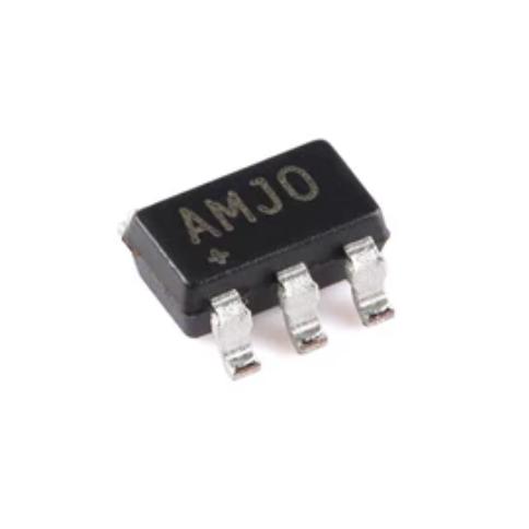
Image for reference only

制造商零件:

MAX40203AUK+T

包装:

SOT-23-5(SC-74A,SOT-753)(2.90 x 1.60 x 1.45 毫米,0.95 毫米间距)

品牌:
产品类别:
您可能感兴趣的其他建议.
说明

The MAX40203AUK+T from Analog Devices (Maxim Integrated) is an ultra-tiny nanoPower 1A ideal diode current switch in a 5-pin SOT-23 package. It provides a forward voltage drop approximately one order of magnitude lower than a Schottky diode. When forward-biased and enabled (EN=HIGH), the device conducts with only 14mV drop at 1mA, 16mV at 100mA, 43mV at 500mA, and 90mV at 1A (WLP package; SOT-23 slightly higher). During short circuit or fast power-up, output current is limited to 2A. The device thermally protects itself and downstream circuitry from overcurrent conditions. Supply voltage: 1.2V to 5.5V. Quiescent current: 300nA typical, 500nA maximum. Reverse leakage when disabled (EN=LOW): less than 10nA typical, blocks up to 6V in either direction. Turn-on delay: 320us. Turn-off delay: 80us. Turn-off reverse threshold: 26mV typical. Enable input (EN): active HIGH, compatible with 1.2V to 5.5V logic. Operating temperature: -40C to +125C. MSL 1. Also available in 4-bump WLP (0.77 x 0.77mm, 0.35mm pitch) as MAX40203ANS+T with even lower forward voltage drop. Active product, RoHS compliant, EAR99.

The MAX40203AUK+T from Analog Devices (Maxim Integrated) is a nanoPower ideal diode current switch that replaces Schottky diodes in power routing applications with dramatically lower forward voltage drop. In a compact 5-pin SOT-23 package, it delivers the functionality of a near-perfect diode with only 90mV of forward drop at 1A, compared to 300-500mV for a typical Schottky diode at the same current. This 3-5x reduction in voltage drop translates directly to longer battery life and cooler operation in portable devices.

The ideal diode concept is straightforward: instead of using a passive P-N junction (Schottky or conventional diode) for power routing, the MAX40203 uses an active MOSFET switch with intelligent control circuitry. An internal comparator monitors the voltage difference between the input (VDD) and output (OUT). When VDD exceeds OUT by a small threshold (indicating forward-bias condition), the MOSFET turns on, allowing current to flow with very low resistance. When OUT exceeds VDD (reverse-bias condition), the MOSFET turns off within 80us, blocking reverse current flow. This behavior mimics a diode but with much lower forward voltage drop and much faster reverse recovery.

The device is particularly valuable in ORing applications where two or more power sources (e.g., main battery and backup battery, or USB and battery) are connected to a common load through separate ideal diodes. The low forward drop ensures that the higher-voltage source supplies the load, while the reverse blocking prevents current from flowing back into the lower-voltage source. With a Schottky diode, the voltage drop at 1A would be 300-500mV, which significantly reduces the usable voltage at the load and wastes power as heat. The MAX40203 reduces this loss by an order of magnitude.

The quiescent current of 300nA is among the lowest for any ideal diode controller, making it suitable for always-on battery-powered devices where even microamp-level quiescent current can drain the battery over time. When disabled (EN=LOW), the device draws even less current and blocks voltages up to 6V in both directions, providing complete isolation of the power path.

The integrated current limiting of 2A protects the device and downstream circuitry during short circuits. If the output is shorted to ground while the device is enabled, the internal current-limit circuit reduces the MOSFET gate drive to limit the output current to approximately 2A. The resulting power dissipation (VDD x 2A) causes the junction temperature to rise, and the thermal protection circuit shuts down the device when the junction temperature exceeds the thermal shutdown threshold (approximately 145C with 14C hysteresis). The device automatically restarts when it cools down.

The EN (enable) pin provides direct control over the ideal diode function. When EN is HIGH (above approximately 1.0V), the ideal diode function is enabled and the device operates normally. When EN is LOW (below approximately 0.4V), the MOSFET is turned off regardless of the VDD-OUT voltage difference, blocking current in both directions. This allows system-level control over power routing, such as disabling a backup battery path when the main supply is active.

The MAX40203AUK+T is the SOT-23-5, tape-and-reel packaged version (2,500 units per reel). The MAX40203AUK+ is the cut-tape version. The MAX40203ANS+T is the 4-bump WLP version (0.77 x 0.77mm) with even lower forward voltage drop, suitable for ultra-compact designs where PCB area is at a premium.

The MAX40203AUK+T operates as an active ideal diode using an internal P-channel MOSFET with intelligent control circuitry.

Internal MOSFET and Controller: The core element is a P-channel MOSFET connected between the VDD (input) and OUT (output) pins. A P-channel MOSFET is used because it can be turned on with a gate voltage lower than the source (VDD), which is naturally available without a charge pump. The MOSFET is sized to carry 1A continuous current with minimal voltage drop. The on-resistance is designed such that at 1A forward current, the voltage drop (VDD – OUT) is approximately 90mV (SOT-23 package).

Forward-Bias Detection: An internal comparator continuously monitors the voltage difference between VDD and OUT. When VDD exceeds OUT by more than the forward turn-on threshold (approximately 10-20mV), the comparator output signals the gate driver to turn on the MOSFET. The MOSFET gate is driven to a voltage that allows the desired forward current to flow. As the load current increases, the gate drive strengthens to maintain the MOSFET in the linear region with controlled voltage drop. At low currents (1mA), the drop is only 14mV; at 1A, the drop increases to approximately 90mV due to the MOSFET on-resistance.

Reverse-Bias Blocking: When OUT exceeds VDD (reverse-bias condition), the comparator detects this within 80us and turns off the MOSFET gate drive. The MOSFET turns off, blocking reverse current flow. The reverse blocking threshold is approximately 26mV (VOUT – VDD), meaning the device turns off when the output voltage exceeds the input by 26mV. Once the MOSFET is off, the reverse leakage current is less than 10nA typical, which is far lower than a Schottky diode (typically 1-100uA at rated voltage). The device blocks voltages up to 6V in the reverse direction.

Enable Control: The EN pin provides an external control input. When EN is driven HIGH (above the enable threshold, approximately 1.0V), the ideal diode function is enabled and the device operates normally. When EN is driven LOW (below the disable threshold, approximately 0.4V), the gate driver is forced off regardless of the VDD-OUT voltage, and the MOSFET is turned off. In the disabled state, the device blocks up to 6V in both directions and draws minimal current from both VDD and EN pins.

Current Limiting: The internal current-limit circuit monitors the MOSFET current. When the forward current exceeds approximately 2A (such as during an output short circuit or a fast power-up into a large capacitive load), the gate drive is reduced to limit the current. The current limit operates in a constant-current mode, maintaining approximately 2A through the MOSFET. The resulting power dissipation (VDD x 2A) causes the junction temperature to rise.

Thermal Protection: When the junction temperature exceeds the thermal shutdown threshold (approximately 145C), the MOSFET is turned off to prevent damage. The thermal shutdown has 14C of hysteresis, meaning the device does not restart until the junction temperature drops to approximately 131C. This thermal cycling continues as long as the overcurrent condition persists, providing self-protection without requiring external intervention. The thermal protection also protects downstream circuitry by limiting the power that can be delivered into a fault.

Low Quiescent Current: The 300nA quiescent current is achieved through the use of sub-threshold CMOS design techniques in the control circuitry. The comparator, bias circuits, and gate driver are all designed to operate at nanoampere current levels. The quiescent current is relatively constant over the load current range because the control circuitry operates independently of the load current path. The low quiescent current ensures minimal battery drain in always-on applications such as backup power systems and portable devices in sleep mode.

针脚 名称 类型 说明
1 EN 输入 Enable input; active HIGH; when HIGH (above ~1.0V), ideal diode function is enabled and the MOSFET operates as a controlled switch; when LOW (below ~0.4V), the MOSFET is forced off and current is blocked in both directions; compatible with 1.2V to 5.5V logic; can be connected directly to VDD for always-enabled operation; internal pulldown ensures device is disabled if pin is left floating
2 接地 地面 Device ground; connect to PCB ground plane; all internal circuitry references this pin; input current monitoring and thermal protection use GND as reference
3 VDD 电源输入 Input supply voltage; 1.2V to 5.5V; connect to the power source being switched (battery, USB, etc.); this is the source terminal of the internal P-channel MOSFET; bypass with 1uF ceramic capacitor to GND close to the device; forward current flows from VDD to OUT when the device is enabled
4 北卡罗来纳州 No Connect Not internally connected; leave floating or tie to GND; this pin exists for package compatibility and has no electrical function
5 出局 功率输出 Output voltage; connects to the load or common power rail; this is the drain terminal of the internal P-channel MOSFET; when the device is forward-biased and enabled, current flows from VDD through the MOSFET to OUT; when reverse-biased or disabled, OUT is isolated from VDD; bypass with 1uF ceramic capacitor to GND
应用 说明
Battery ORing / Power Source Selection Connect main battery and backup battery through separate MAX40203 devices to a common load rail; the source with higher voltage automatically supplies the load; reverse blocking prevents backfeeding from the higher-voltage source to the lower-voltage source; 90mV drop at 1A vs 300-500mV for Schottky extends battery life by 5-15%; EN pin allows system-level power source switching
USB / Battery Power Routing Route power from USB or internal battery to device load; when USB is connected (5V), it supplies the load through the ideal diode; when USB is disconnected, the battery (3.7V Li-ion) takes over seamlessly; low 300nA quiescent current minimizes battery drain during USB operation; reverse blocking prevents battery backfeed into USB port
Notebook / Tablet Power Management Replace Schottky diodes in notebook power path ORing; 90mV drop reduces power dissipation from 500mW to 90mW at 1A, eliminating need for heat sinking; lower voltage drop provides more margin for low-voltage CPU core rails; thermal self-protection replaces external fuse in some designs
Portable Medical Device Battery Backup OR primary battery with backup battery in medical devices; ultra-low 10nA reverse leakage prevents battery cross-drain; thermal protection ensures safe operation during fault conditions; wide -40C to +125C temperature range for medical environments; EN pin allows disabling backup path for battery conservation
Solar / Energy Harvesting Prevent reverse current from storage capacitor back through solar cell at night; 90mV forward drop maximizes energy harvested from low-voltage solar cells; 10nA reverse leakage minimizes nighttime energy loss; 1.2V minimum VDD supports single-cell solar output
模型 制造商 兼容性 主要区别
MAX40203ANS+T ADI Same in WLP Package Same ideal diode function in 4-bump WLP (0.77 x 0.77mm, 0.35mm pitch); even lower forward voltage drop (14mV at 1mA, 43mV at 500mA); no EN pin (always enabled); use for ultra-compact designs where SOT-23 is too large
MAX40200AUK+T ADI Similar, Lower Current 500mA ideal diode in same SOT-23-5 pinout; lower forward drop at 500mA (43mV vs 43mV similar); lower current limit; use for lower-current applications where 500mA is sufficient
LM66100DCKT TI 功能相似 Dual ideal diode in SOT-6 (SC-88); 1.5A per channel; 1.5-5.5V supply; two independent ideal diodes in one package; different pinout; higher quiescent current (1.5uA); use when two ORing paths are needed
TPS22916DBVR TI Load Switch Alternative 1A load switch in SOT-23-5; 1.0-5.5V; 80mOhm RDS(on); no ideal diode function (unidirectional only); active-high enable; use when only unidirectional switching is needed without reverse blocking
MBR120VLSFT1G ON 半 Schottky Alternative 1A Schottky diode in SOD-123; 20V; 340mV forward drop at 1A; passive device (no control); no enable function; much higher voltage drop than MAX40203; simplest and lowest cost but least efficient
推荐部件
3-16S battery monitor/protector, Li-Ion/LiFePO4, 2 ADCs, TQFP-48

品牌:

封装:

TQFP-48 (7 x 7 x 1.0 mm)
有库存:
2150pcs

货运周期:3~7 天
最低订购量为 1

转到查询
I2C 4.5A 1-cell Li-ion charger, NVDC power path, USB OTG, VQFN-24

品牌:

封装:

VQFN-24 (4.0 x 4.0 x 0.75 mm, with thermal pad)
有库存:
4182pcs

货运周期:3~7 天
最低订购量为 1

转到查询
Single micropower RRIO op-amp, 2.7-10V, 65kHz, 11uA, SOT-23-5

品牌:

封装:

SOT-23-5 (2.9 x 2.8 x 1.15 mm)
有库存:
8750pcs

货运周期:3~7 天
最低订购量为 1

转到查询
Single 2-input AND gate, 1.65-5.5V, 24mA drive, SOT-23-5, LVC

品牌:

封装:

SOT-23-5 (2.9 x 1.6 x 1.15 mm)
有库存:
35000 件

货运周期:3~7 天
最低订购量为 1

转到查询
8-bit parallel-load shift register, PISO, 2-6V, 24 MHz, SOIC-16

品牌:

封装:

SOIC-16 (9.9 x 6.0 mm)
有库存:
4837pcs

货运周期:3~7 天
最低订购量为 1

转到查询
Quad differential line receiver, EIA-422/423, 3-state TTL outputs, 5V, SOIC-16

品牌:

封装:

SOIC-16 (9.9 x 6.0 mm)
有库存:
0 件

货运周期:3~7 天
最低订购量为 1

转到查询
质量保证

我们从合作供应链采购的所有电子元件都经过严格的进货检验。通过仔细的测试,我们确保交付给客户的所有产品都是原装正品,符合质量要求。此外,我们还保存完整的检验记录,使整个供应链流程清晰可查。.

认证
我们获得了多项专业认证,并建立了自己的专业检测实验室,确保交付给客户的每一件产品都符合最高质量要求。我们严格按照流程进行检测,确保产品质量稳定、参数准确。为保证原装正品,我们还与可靠的第三方检测机构合作,进行严格的质量检测。我们始终高度重视质量,完全符合行业标准、相关法规和 ISO 9001:2015 的要求。.

发货与付款

我们从合作供应链采购的所有电子元件都经过严格的进货检验。通过仔细的测试,我们确保交付给客户的所有产品都是原装正品,符合质量要求。此外,我们还保存完整的检验记录,使整个供应链流程清晰可查。.

认证
我们获得了多项专业认证,并建立了自己的专业检测实验室,确保交付给客户的每一件产品都符合最高质量要求。我们严格按照流程进行检测,确保产品质量稳定、参数准确。为保证原装正品,我们还与可靠的第三方检测机构合作,进行严格的质量检测。我们始终高度重视质量,完全符合行业标准、相关法规和 ISO 9001:2015 的要求。.

服务与包装

我们从合作供应链采购的所有电子元件都经过严格的进货检验。通过仔细的测试,我们确保交付给客户的所有产品都是原装正品,符合质量要求。此外,我们还保存完整的检验记录,使整个供应链流程清晰可查。.

认证
我们获得了多项专业认证,并建立了自己的专业检测实验室,确保交付给客户的每一件产品都符合最高质量要求。我们严格按照流程进行检测,确保产品质量稳定、参数准确。为保证原装正品,我们还与可靠的第三方检测机构合作,进行严格的质量检测。我们始终高度重视质量,完全符合行业标准、相关法规和 ISO 9001:2015 的要求。.



