首页 > 集成电路 IC > LM2901DR

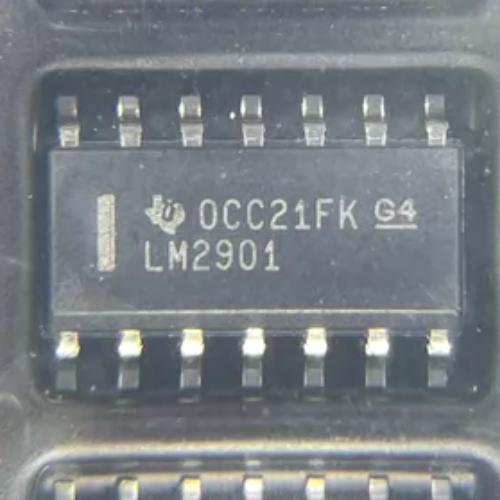
LM2901DR


四路比较器,2-30V,集电极开路输出,1.3us prop 延迟,7mV Vos,CM 输入(包括接地端),SOIC-14,-40~125C,卷带包装

80000

有效库存
转到查询

Image for reference only

制造商零件:

LM2901DR

包装:

SOIC-14 (D)(8.65 x 6.0 毫米,1.27 毫米间距)

品牌:
产品类别:
您可能感兴趣的其他建议.
说明

The LM2901DR from Texas Instruments is a quad differential comparator operating from a single 2 V to 30 V supply in an SOIC-14 (D) package (8.65 x 6 mm). Key specifications: four independent voltage comparators; open-collector/open-drain output; 1.3 us typical propagation delay; input offset voltage 7 mV max at 25 degrees C; input bias current 250 nA max; common-mode input voltage range includes ground (0 V to 28.5 V); differential input voltage range equal to maximum-rated supply voltage plus or minus 38 V; low output saturation voltage; output compatible with TTL, MOS, and CMOS; quiescent current 0.2 mA per comparator typical; operating temperature -40 to +125 degrees C. The LM2901B is an upgraded drop-in replacement with 0.37 mV offset, 3.5 nA bias current, 1 us response time, and 38 V max supply. The D suffix denotes SOIC-14 package, R suffix denotes tape and reel. RoHS compliant.

The LM2901DR from Texas Instruments is the automotive/industrial-qualified version of the industry-standard LM339 quad differential comparator family. It contains four independent voltage comparators in a single SOIC-14 package, designed to operate from a single power supply over a wide voltage range of 2 V to 30 V without requiring a dual supply.

The LM2901 is one of the most widely used comparators in the electronics industry, alongside its commercial-grade sibling the LM339. The primary difference is the extended operating temperature range: the LM2901 is specified for -40 to +125 degrees C (automotive grade), while the LM339 is specified for 0 to +70 degrees C (commercial grade). The LM2901 also has slightly relaxed offset voltage and bias current specifications to account for the wider temperature range.

The open-collector output architecture is a defining feature. Each comparator output is an NPN transistor with an open collector, meaning the output can only pull low (sink current to ground) but cannot pull high. An external pull-up resistor is required to establish the high logic level. This has several advantages: (1) the output can be pulled up to a voltage different from the comparator supply (wired-OR logic); (2) multiple open-collector outputs can be connected together to implement AND or NOR logic without additional gates; (3) the output can directly drive loads such as LEDs, relays, or optocouplers.

The common-mode input voltage range that includes ground (0 V) is critical for single-supply applications. Many comparators require the inputs to be at least 1-2 V above the negative rail, but the LM2901 allows both inputs to go to ground (or even slightly below) without phase inversion or output glitches. This makes it ideal for low-side current sensing, battery monitoring, and zero-crossing detection applications where the input signal may be near ground.

The differential input voltage range of plus or minus 38 V (for the B-version) exceeds the supply voltage range, meaning the two inputs can differ by up to 38 V without damaging the device. This is useful for comparing signals from different voltage domains, such as monitoring a 24 V industrial signal with a 5 V comparator supply.

TI offers the LM2901B as an upgraded drop-in replacement with significantly improved specifications: offset voltage reduced from 7 mV to 0.37 mV (19x improvement), input bias current from 250 nA to 3.5 nA (71x improvement), propagation delay from 1.3 us to 1 us, and ESD rating from 500 V to 2 kV HBM. For new designs, TI recommends the B-version. However, the original LM2901 remains in high-volume production due to its extremely low cost and established design heritage.

The LM2901DR is available in SOIC-14 with tape and reel packaging (R suffix), suitable for automated SMT assembly. Other package options include PDIP-14 (N suffix), TSSOP-14 (PW suffix), and SOP-14 (NS suffix).

The LM2901DR operates as four independent differential voltage comparators sharing a common power supply and ground.

Comparator Operation: Each comparator has two inputs (IN+ and IN-) and one open-collector output. The comparator continuously compares the voltage at the non-inverting input (IN+) with the voltage at the inverting input (IN-). When V(IN+) is greater than V(IN-) by at least the offset voltage plus the overdrive voltage, the output transistor is off (open collector), and the output is pulled high by an external pull-up resistor. When V(IN+) is less than V(IN-), the output transistor turns on, pulling the output low (saturating to near ground). The output state changes when the differential input voltage crosses the switching threshold, which is ideally zero but is affected by the input offset voltage (up to 7 mV).

Open-Collector Output: The output stage consists of an NPN transistor with its collector connected to the output pin and its emitter connected to ground. When the comparator detects that IN+ is less than IN-, the output transistor saturates, pulling the output pin toward ground (typically 0.25 V at 4 mA sink current). When IN+ is greater than IN-, the output transistor is off, and the output pin floats (high impedance). An external pull-up resistor (typically 1 kOhm to 100 kOhm) connected from the output pin to the logic supply voltage establishes the high logic level. The pull-up voltage can be different from the comparator supply voltage, allowing level shifting.

Input Stage: The input stage uses a PNP differential pair that allows the common-mode input voltage range to extend down to ground (0 V) and up to VCC – 1.5 V. The PNP input transistors source a small bias current (typically 25 nA, max 250 nA) that flows out of the input pins. This bias current must be considered when designing high-impedance input networks, as it can create voltage offsets across source resistances. The differential input voltage is clamped by back-to-back diodes in parallel with a 1 kOhm resistor, limiting the differential current to safe levels even when the input voltage difference exceeds the supply voltage.

Propagation Delay: The typical propagation delay is 1.3 us for a 100 mV input step with 5 mV overdrive. This is relatively slow compared to dedicated high-speed comparators (which can be 10-100 ns), but is adequate for most control and monitoring applications. The propagation delay increases with smaller overdrive voltages and larger load capacitances.

Wired-OR Configuration: Multiple open-collector outputs can be connected together to a single pull-up resistor to implement a wired-OR (actually wired-AND) function. If any comparator output is low, the combined output is low. This is useful for creating multi-channel window comparators or multi-input alarm circuits without additional logic gates.

Power Supply: The LM2901 operates from a single supply (VCC to GND) without requiring a negative supply. The quiescent current is approximately 0.8 mA total (0.2 mA per comparator) and is relatively independent of supply voltage. The comparators remain functional down to 2 V supply, making them suitable for battery-powered applications.

针脚 名称 类型 说明
1 OUT2 输出 Comparator 2 open-collector output; pulls low (saturates to ground) when IN2- is greater than IN2+; floats high-impedance when IN2+ is greater than IN2-; requires external pull-up resistor to establish high logic level; can be pulled up to any voltage up to 30 V (independent of VCC); can sink up to 16 mA continuous; saturation voltage typically 0.25 V at 4 mA
2 OUT1 输出 Comparator 1 open-collector output; same characteristics as OUT2; can be wire-ORed with other outputs
3 VCC 电源 Positive supply voltage; 2 V to 30 V; bypass with 100 nF ceramic capacitor to GND; quiescent current approximately 0.8 mA total for all four comparators; current does not vary significantly with supply voltage
4 IN1- 输入 Comparator 1 inverting input; common-mode voltage range 0 V to VCC-1.5 V; input bias current typically 25 nA flowing out of the pin; differential input voltage range plus or minus 38 V (B-version); this pin sets the reference voltage for comparator 1
5 IN1+ 输入 Comparator 1 non-inverting input; same voltage range and bias current as IN1-; when IN1+ voltage exceeds IN1- voltage, the output is high (open circuit)
6 IN2- 输入 Comparator 2 inverting input; same characteristics as IN1-; independent of comparator 1
7 IN2+ 输入 Comparator 2 non-inverting input; same characteristics as IN1+
8 IN3- 输入 Comparator 3 inverting input; same characteristics as IN1-
9 IN3+ 输入 Comparator 3 non-inverting input; same characteristics as IN1+
10 IN4- 输入 Comparator 4 inverting input; same characteristics as IN1-
11 IN4+ 输入 Comparator 4 non-inverting input; same characteristics as IN1+
12 接地 地面 Ground; the negative supply rail; the common-mode input range includes this voltage (0 V); all output transistors sink current to this pin; connect to PCB ground plane
13 OUT4 输出 Comparator 4 open-collector output; same characteristics as OUT2
14 OUT3 输出 Comparator 3 open-collector output; same characteristics as OUT2
应用 说明
电池低电压检测器 Use one comparator to monitor battery voltage against a reference set by a voltage divider and zener; open-collector output drives LED indicator or MCU interrupt; common-mode range includes ground for low-side monitoring; wide supply range (2-30 V) allows direct operation from the battery; 125 degrees C rated for under-hood automotive use
窗口比较器 Use two comparators to create a window detector: one detects overvoltage (IN+ above upper threshold) and one detects undervoltage (IN+ below lower threshold); wire-OR the open-collector outputs to create a single fault output that is low when the input is outside the acceptable window; ideal for power supply monitoring
零交叉探测器 Detect when an AC signal crosses zero volts; one comparator with IN- at ground and IN+ connected to the AC signal through a current-limiting resistor; output transitions at each zero crossing; useful for TRIAC/SSR firing angle control, dimmer circuits, and frequency measurement
Motor Overcurrent Protection Compare current-sense amplifier output against a reference voltage; when the motor current exceeds the threshold, the comparator output drives a shutdown signal; open-collector output can drive MOSFET gate or enable pin directly; fast 1.3 us response time enables rapid fault detection
Thermostat / Temperature Control Compare NTC thermistor voltage divider output against a setpoint reference; one comparator for heating (turn on when below setpoint) and one for cooling (turn on when above setpoint); open-collector outputs drive relay drivers or TRIAC optocouplers; hysteresis added with feedback resistor
模型 制造商 兼容性 主要区别
LM2901BDR TI Drop-in Upgrade Same pinout and package; improved specifications: 0.37 mV offset (vs 7 mV), 3.5 nA bias (vs 250 nA), 1 us response (vs 1.3 us), 2 kV ESD (vs 500 V), 38 V max (vs 30 V); recommended for new designs; slightly higher cost
LM339DR TI Pin-Compatible, Commercial Same quad comparator in SOIC-14; commercial temperature range 0 to 70 degrees C (vs -40 to 125 C); lower offset voltage 2 mV typical; use when extended temperature is not needed and lower offset is desired
LM393DR TI Dual Version Dual (not quad) comparator in SOIC-8; same comparator architecture; two comparators instead of four; smaller package; use when only two comparators are needed and board space is limited
TL331BDBVR TI Single Version Single B-version comparator in SOT-23-5; improved specifications; smallest footprint; use when only one comparator is needed and space is critical
TSX3704IDT ST Push-Pull Alternative Quad comparator with push-pull CMOS output (no pull-up resistor needed); rail-to-rail input; 2.7-16 V supply; faster response time; use when open-collector is not needed and simpler output is preferred
推荐部件
PMIC for AM335x, 3 DC-DC, 4 LDO, Li-ion charger, WLED driver, VQFN-48

品牌:

封装:

VQFN-48 (6 x 6 x 0.9 mm, 0.4 mm pitch, with thermal pad)
有库存:
4012pcs

货运周期:3~7 天
最低订购量为 1

转到查询
Octal D-type flip-flop with clear, 2-6V, 28 MHz, SOP-20

品牌:

封装:

SOP-20 NS (10.2 x 5.3 mm)
有库存:
7821pcs

货运周期:3~7 天
最低订购量为 1

转到查询
3-to-8 line decoder/demux, active-low outputs, 2-6V, PDIP-16

品牌:

封装:

PDIP-16 (19.3 x 6.35 mm)
有库存:
10248pcs

货运周期:3~7 天
最低订购量为 1

转到查询
2W mono Class-AB audio amp, BTL/SE, 2.5-5.5V, HVSSOP-8 PowerPAD

品牌:

封装:

HVSSOP-8 (DGN) with PowerPAD (4.9 x 3.9 mm)
有库存:
9105pcs

货运周期:3~7 天
最低订购量为 1

转到查询
10/100 Ethernet PHY transceiver, MII/RMII/SNI, 3.3V, LQFP-48, commercial temp

品牌:

封装:

LQFP-48 (7 x 7 mm)
有库存:
5472pcs

货运周期:3~7 天
最低订购量为 1

转到查询
Octal bus transceiver, 3-state outputs, 2-6V, 8-channel, TSSOP-20

品牌:

封装:

TSSOP-20 (6.5 x 4.4 mm)
有库存:
7654pcs

货运周期:3~7 天
最低订购量为 1

转到查询
质量保证

我们从合作供应链采购的所有电子元件都经过严格的进货检验。通过仔细的测试,我们确保交付给客户的所有产品都是原装正品,符合质量要求。此外,我们还保存完整的检验记录,使整个供应链流程清晰可查。.

认证
我们获得了多项专业认证,并建立了自己的专业检测实验室,确保交付给客户的每一件产品都符合最高质量要求。我们严格按照流程进行检测,确保产品质量稳定、参数准确。为保证原装正品,我们还与可靠的第三方检测机构合作,进行严格的质量检测。我们始终高度重视质量,完全符合行业标准、相关法规和 ISO 9001:2015 的要求。.

发货与付款

我们从合作供应链采购的所有电子元件都经过严格的进货检验。通过仔细的测试,我们确保交付给客户的所有产品都是原装正品,符合质量要求。此外,我们还保存完整的检验记录,使整个供应链流程清晰可查。.

认证
我们获得了多项专业认证,并建立了自己的专业检测实验室,确保交付给客户的每一件产品都符合最高质量要求。我们严格按照流程进行检测,确保产品质量稳定、参数准确。为保证原装正品,我们还与可靠的第三方检测机构合作,进行严格的质量检测。我们始终高度重视质量,完全符合行业标准、相关法规和 ISO 9001:2015 的要求。.

服务与包装

我们从合作供应链采购的所有电子元件都经过严格的进货检验。通过仔细的测试,我们确保交付给客户的所有产品都是原装正品,符合质量要求。此外,我们还保存完整的检验记录,使整个供应链流程清晰可查。.

认证
我们获得了多项专业认证,并建立了自己的专业检测实验室,确保交付给客户的每一件产品都符合最高质量要求。我们严格按照流程进行检测,确保产品质量稳定、参数准确。为保证原装正品,我们还与可靠的第三方检测机构合作,进行严格的质量检测。我们始终高度重视质量,完全符合行业标准、相关法规和 ISO 9001:2015 的要求。.



