首页 > 集成电路 IC > DRV8833CRTER

DRV8833CRTER


双 H 桥电机驱动器,2.7-10.8V,0.6A RMS/1A 峰值(WQFN),PWM 电流调节,已停用,用 DRV8410/8411 代替

0

有效库存
转到查询

Image for reference only

制造商零件:

DRV8833CRTER

包装:

WQFN-16(RTE),带 PowerPAD(3.00 x 3.00 x 0.75 毫米)

品牌:
产品类别:
您可能感兴趣的其他建议.
说明

The DRV8833CRTER from Texas Instruments is a dual H-bridge motor driver in a 16-pin WQFN (RTE) package with PowerPAD (3.00 x 3.00 mm). It is the C-version of the DRV8833 with integrated current regulation capability. NOTE: This device is OBSOLETE and no longer in production. TI recommends the DRV8410RTER or DRV8411RTER as direct replacements (same pinout, same package, enhanced features). The DRV8833C can drive two DC brush motors or one bipolar stepper motor. Motor supply voltage: 2.7V to 10.8V. Output current per H-bridge: 0.6A RMS / 1A peak in WQFN package (lower than HTSSOP due to thermal constraints). MOSFET on-resistance: HS+LS = 1735mOhm typical at 5V/25C (higher than DRV8833 due to different MOSFET sizing in C-version). Integrated PWM current regulation via external sense resistors on AISEN/BISEN pins. Simple PWM interface: 4 logic inputs (AIN1, AIN2, BIN1, BIN2) control motor direction and brake. nSLEEP pin for low-power sleep mode (1.6uA typical). nFAULT open-drain output for overcurrent, short-circuit, UVLO, and thermal shutdown fault reporting. Internal charge pump for high-side gate drive (0.01uF cap between VCP and VM). VINT internal 3.3V regulator bypass (2.2uF cap to GND). Operating temperature: -40C to +85C. RoHS compliant.

The DRV8833CRTER from Texas Instruments is a dual H-bridge motor driver with integrated PWM current regulation, housed in a compact 16-pin WQFN package with PowerPAD for thermal management. It is designed for battery-powered toys, printers, security cameras, and other mechatronic applications requiring precise motor control.

IMPORTANT: This device is OBSOLETE and no longer in production. Texas Instruments recommends the DRV8410RTER (2.5A, same pinout) or DRV8411RTER (4A, same pinout) as direct replacements. The DRV8410/8411 are drop-in compatible with enhanced current capability and extended temperature range (-40C to +125C).

The DRV8833C is the current-regulated variant of the DRV8833 family. The key difference from the standard DRV8833 is the addition of PWM current regulation circuitry that uses external sense resistors on the AISEN and BISEN pins to set the current regulation threshold. This allows precise control of motor winding current, which is essential for stepper motor applications where accurate current setting determines torque and microstepping accuracy.

Each H-bridge consists of N-channel and P-channel MOSFETs in a standard H-bridge configuration. The combined high-side and low-side on-resistance (HS+LS) is 1735mOhm typical at 5V/25C, which is significantly higher than the DRV8833 (360mOhm). This higher resistance reduces the current capacity of the DRV8833C in the WQFN package to 0.6A RMS per bridge, compared to 1.5A RMS for the DRV8833 in the HTSSOP package.

The PWM current regulation works by monitoring the voltage across the external sense resistor (connected between AISEN/BISEN and GND). When the voltage exceeds the internal 200mV reference, the driver enters a fast-decay mode for a fixed off-time, reducing the average current through the motor winding. The current regulation threshold is set by the sense resistor value: I_trip = 0.2V / R_sense. For example, a 0.33Ohm resistor sets the trip current to approximately 606mA.

The device is controlled through four logic inputs (AIN1, AIN2, BIN1, BIN2) that directly set the state of the corresponding outputs. This simple PWM interface requires no serial communication or register programming. Each pair of inputs controls one H-bridge: when xIN1=HIGH and xIN2=LOW, current flows forward through the motor; when xIN1=LOW and xIN2=HIGH, current flows in reverse; when both inputs are LOW or both HIGH, the motor brakes. PWM signals on the input pins control motor speed.

The nSLEEP pin provides a low-power sleep mode that reduces the supply current to 1.6uA typical. When nSLEEP is driven low, all internal circuitry including the charge pump is disabled, and the outputs are placed in a high-impedance state. When nSLEEP returns high, the device wakes up in approximately 155us.

Protection features include overcurrent protection (OCP) that limits current through the MOSFETs to a safe level, undervoltage lockout (UVLO) that disables the outputs when VM drops below the threshold, thermal shutdown (TSD) that disables the outputs when the junction temperature exceeds approximately 150C, and short-circuit protection. All fault conditions are reported through the nFAULT open-drain output.
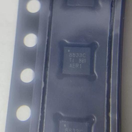

The DRV8833CRTER operates as a dual H-bridge motor driver with integrated PWM current regulation.

H-Bridge Architecture: Each of the two H-bridges consists of four power MOSFETs arranged in an H-configuration. The high-side MOSFETs are P-channel devices (for simpler gate drive), and the low-side MOSFETs are N-channel devices. The H-bridge allows bidirectional current flow through the motor winding: when the upper-left and lower-right MOSFETs are on, current flows in one direction; when the upper-right and lower-left MOSFETs are on, current flows in the opposite direction.

Charge Pump and Gate Drive: An internal charge pump generates the gate drive voltage for the high-side N-channel MOSFETs (note: the DRV8833 uses N-channel MOSFETs for both high and low side, unlike the DRV8833C which uses a mix of N and P channels). A 0.01uF capacitor connected between VCP and VM stores the charge pump output. The charge pump operates at a fixed frequency and provides sufficient gate drive even at low supply voltages (2.7V).

PWM Current Regulation: The DRV8833C adds current regulation capability not present in the standard DRV8833. External sense resistors (R_sense) are connected between the AISEN/BISEN pins and GND. The voltage across the sense resistor is proportional to the motor current: V_sense = I_motor x R_sense. An internal comparator compares V_sense to a 200mV reference voltage. When V_sense exceeds 200mV (indicating the motor current has exceeded the set threshold), the driver enters a fast-decay mode for a fixed off-time period, turning off the appropriate MOSFETs and allowing the current to recirculate through the freewheeling diodes. After the off-time expires, the MOSFETs are re-enabled, and the cycle repeats. This chopper-style regulation maintains the average motor current at the set level regardless of supply voltage variations or back-EMF changes.

Logic Control: The AIN1/AIN2 and BIN1/BIN2 inputs directly control the H-bridge output states through a simple logic decoder. When xIN1=1 and xIN2=0: xOUT1=HIGH, xOUT2=LOW (forward). When xIN1=0 and xIN2=1: xOUT1=LOW, xOUT2=HIGH (reverse). When xIN1=0 and xIN2=0: both outputs high-impedance (coast/fast decay). When xIN1=1 and xIN2=1: both outputs LOW (brake/slow decay). PWM speed control is achieved by rapidly switching between the forward (or reverse) state and the coast or brake state.

Internal Regulator: The VINT pin provides access to the internal 3.3V regulator output, which powers the logic and control circuitry. A 2.2uF bypass capacitor is required on the VINT pin to ensure stable regulator operation. The internal regulator allows the device to operate from a single supply (VM) without a separate logic supply.

Fault Protection: The overcurrent protection (OCP) circuit monitors the current through each MOSFET independently. If the current exceeds the safe operating limit (approximately 2-3A depending on conditions), the driver immediately disables the affected H-bridge and asserts nFAULT. The thermal shutdown circuit monitors the junction temperature and disables both H-bridges when it exceeds approximately 150C. The undervoltage lockout (UVLO) disables the outputs when VM drops below approximately 2.5V. All fault conditions are reported through the nFAULT open-drain output, which requires an external pull-up resistor.

Pin (RTE) 名称 类型 说明
1 AISEN 输入/输出 Bridge A current sense; connect external sense resistor to GND for PWM current regulation (I_trip = 0.2V/R_sense); connect directly to GND if current regulation is not needed
2 AOUT2 输出 Bridge A output 2; connect to motor winding A
3 BOUT2 输出 Bridge B output 2; connect to motor winding B
4 BISEN 输入/输出 Bridge B current sense; connect external sense resistor to GND for PWM current regulation; connect directly to GND if not needed
5 BOUT1 输出 Bridge B output 1; connect to motor winding B
6 nFAULT Open-Drain Output Fault indicator; active-low open-drain; asserts during overcurrent, short-circuit, UVLO, or overtemperature; requires external pull-up resistor (10kOhm typical)
7 BIN1 输入 Bridge B input 1; logic input controls BOUT1 state; internal pulldown resistor (100-150kOhm); compatible with 3.3V and 5V logic
8 BIN2 输入 Bridge B input 2; logic input controls BOUT2 state; internal pulldown
9 VCP 输入/输出 Charge pump output; connect 0.01uF ceramic capacitor (16V minimum, X7R) between VCP and VM; provides gate drive voltage for high-side MOSFETs
10 VM 电源 Motor power supply input; 2.7V to 10.8V; bypass to GND with 10uF (minimum) ceramic capacitor rated for maximum VM
11 接地 地面 Device ground; must connect PowerPAD to GND for proper thermal and electrical operation
12 VINT 电源 Internal 3.3V regulator output; bypass to GND with 2.2uF, 6.3V ceramic capacitor; do not use to power external circuitry
13 AIN2 输入 Bridge A input 2; logic input controls AOUT2 state; internal pulldown
14 AIN1 输入 Bridge A input 1; logic input controls AOUT1 state; internal pulldown
15 nSLEEP 输入 Sleep mode input; logic HIGH = normal operation; logic LOW = low-power sleep mode (1.6uA typical); internal pulldown ensures sleep mode if pin floats; wake-up time approximately 155us
16 AOUT1 输出 Bridge A output 1; connect to motor winding A; positive current direction is AOUT1 to AOUT2
PPAD PowerPAD 地面 Exposed thermal pad; must be soldered to PCB ground plane for thermal dissipation; electrically connected to GND internally
应用 说明
Robot Motor Drive (Replacement) Replace failed DRV8833CRTER in existing robot designs; DRV8410RTER is the recommended drop-in replacement with same pinout and 2.5A capability; higher current allows driving larger motors in the same PCB footprint
Battery-Powered Toy Motor Control Drive two small DC motors from 2.7V to 10.8V battery supply; PWM current regulation prevents motor stall damage; low 1.6uA sleep current preserves battery life during idle; simple 4-pin logic interface reduces microcontroller I/O requirements
POS Printer Stepper Motor Drive a bipolar stepper motor for paper feed and print head positioning; PWM current regulation sets precise winding current for consistent step accuracy; nFAULT output enables fault-tolerant operation with automatic error reporting
Security Camera Pan/Tilt Drive two DC motors for pan and tilt axes; 2.7V minimum supply allows operation from single Li-ion cell; compact WQFN-16 package minimizes PCB area in camera housing
Existing Board Maintenance Source DRV8833CRTER for repair of existing products that use this device; for new designs, migrate to DRV8410RTER or DRV8411RTER for improved availability and performance
模型 制造商 兼容性 主要区别
DRV8410RTER TI Drop-In Replacement (Recommended) Same WQFN-16 (RTE) pinout; 2.5A output (vs 0.6A RMS); 1.65V to 11V supply range; same current regulation feature; -40C to +125C temperature range; Active product; recommended for both new designs and replacement of DRV8833CRTER
DRV8411RTER TI Drop-In Replacement (Higher Current) Same WQFN-16 (RTE) pinout; 4A output with IPROPI current sense output; 1.65V to 11V supply range; -40C to +125C temperature range; Active product; use when maximum current is needed
DRV8833PWPR TI Same Family, Different Package DRV8833 (non-C version) in HTSSOP-16; no PWM current regulation; lower RDS(on) = 360mOhm; 1.5A RMS per bridge; larger package (5×6.4mm) but better thermal performance; Active product
DRV8833RTYR TI Same Family, Different Package DRV8833 (non-C version) in WQFN-16 (4x4mm); no PWM current regulation; lower RDS(on); 1.5A RMS; Active product; larger QFN package than RTE
TB6612FNG 东芝 功能相似 Dual H-bridge motor driver; 1.2A continuous per channel; 2.5-13.5V supply; different pinout (SSOP-24); built-in thermal shutdown; no current regulation; widely used alternative
推荐部件
PMIC for AM335x, 3 DC-DC, 4 LDO, Li-ion charger, WLED driver, VQFN-48

品牌:

封装:

VQFN-48 (6 x 6 x 0.9 mm, 0.4 mm pitch, with thermal pad)
有库存:
4012pcs

货运周期:3~7 天
最低订购量为 1

转到查询
Octal D-type flip-flop with clear, 2-6V, 28 MHz, SOP-20

品牌:

封装:

SOP-20 NS (10.2 x 5.3 mm)
有库存:
7821pcs

货运周期:3~7 天
最低订购量为 1

转到查询
3-to-8 line decoder/demux, active-low outputs, 2-6V, PDIP-16

品牌:

封装:

PDIP-16 (19.3 x 6.35 mm)
有库存:
10248pcs

货运周期:3~7 天
最低订购量为 1

转到查询
2W mono Class-AB audio amp, BTL/SE, 2.5-5.5V, HVSSOP-8 PowerPAD

品牌:

封装:

HVSSOP-8 (DGN) with PowerPAD (4.9 x 3.9 mm)
有库存:
9105pcs

货运周期:3~7 天
最低订购量为 1

转到查询
10/100 Ethernet PHY transceiver, MII/RMII/SNI, 3.3V, LQFP-48, commercial temp

品牌:

封装:

LQFP-48 (7 x 7 mm)
有库存:
5472pcs

货运周期:3~7 天
最低订购量为 1

转到查询
Octal bus transceiver, 3-state outputs, 2-6V, 8-channel, TSSOP-20

品牌:

封装:

TSSOP-20 (6.5 x 4.4 mm)
有库存:
7654pcs

货运周期:3~7 天
最低订购量为 1

转到查询
质量保证

我们从合作供应链采购的所有电子元件都经过严格的进货检验。通过仔细的测试,我们确保交付给客户的所有产品都是原装正品,符合质量要求。此外,我们还保存完整的检验记录,使整个供应链流程清晰可查。.

认证
我们获得了多项专业认证,并建立了自己的专业检测实验室,确保交付给客户的每一件产品都符合最高质量要求。我们严格按照流程进行检测,确保产品质量稳定、参数准确。为保证原装正品,我们还与可靠的第三方检测机构合作,进行严格的质量检测。我们始终高度重视质量,完全符合行业标准、相关法规和 ISO 9001:2015 的要求。.

发货与付款

我们从合作供应链采购的所有电子元件都经过严格的进货检验。通过仔细的测试,我们确保交付给客户的所有产品都是原装正品,符合质量要求。此外,我们还保存完整的检验记录,使整个供应链流程清晰可查。.

认证
我们获得了多项专业认证,并建立了自己的专业检测实验室,确保交付给客户的每一件产品都符合最高质量要求。我们严格按照流程进行检测,确保产品质量稳定、参数准确。为保证原装正品,我们还与可靠的第三方检测机构合作,进行严格的质量检测。我们始终高度重视质量,完全符合行业标准、相关法规和 ISO 9001:2015 的要求。.

服务与包装

我们从合作供应链采购的所有电子元件都经过严格的进货检验。通过仔细的测试,我们确保交付给客户的所有产品都是原装正品,符合质量要求。此外,我们还保存完整的检验记录,使整个供应链流程清晰可查。.

认证
我们获得了多项专业认证,并建立了自己的专业检测实验室,确保交付给客户的每一件产品都符合最高质量要求。我们严格按照流程进行检测,确保产品质量稳定、参数准确。为保证原装正品,我们还与可靠的第三方检测机构合作,进行严格的质量检测。我们始终高度重视质量,完全符合行业标准、相关法规和 ISO 9001:2015 的要求。.



