CD4047BM


CMOS monostable/astable multivibrator, 3V-18V, SOIC-14, retriggerable, edge-triggered

3500

有效库存
转到查询

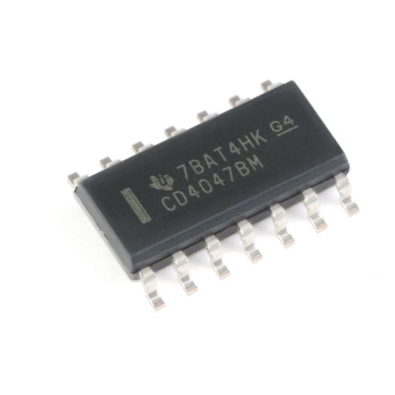
Image for reference only

制造商零件:

CD4047BM

包装:

SOIC-14 (8.65 x 3.9 x 1.5 mm)

品牌:
您可能感兴趣的其他建议.
说明

The CD4047BM is a CMOS monostable/astable multivibrator from TI in SOIC-14 (8.65×3.9mm). Operates in monostable (one-shot) or astable (free-running) modes with single external R and C. Timing: T=2.48RC (monostable Q output), T=4.40RC (astable period). Supply: 3V-18V. Features positive/negative edge trigger, retrigger input, master reset, and complementary Q/Q-bar outputs. 50% duty cycle in astable mode. Ultra-low static current: 0.02uA at 5V. 45% VDD noise immunity. Rise/fall time: 65ns at 10V. -55°C to +125°C. RoHS compliant. Pin-compatible with HEF4047B and CD4047B variants from other manufacturers.

The CD4047BM is a CMOS monostable/astable multivibrator from Texas Instruments, capable of operating in both monostable (one-shot) and astable (free-running) modes with a single external resistor and capacitor. It is a member of the CD4000B CMOS logic family and is housed in a 14-pin SOIC package.

The device provides excellent stability over the full supply voltage range of 3V to 18V and the full military temperature range of -55°C to +125°C. The timing is primarily controlled by an external resistor (R) and capacitor (C), with the pulse width in monostable mode given by T = 2.48RC (positive output) or T = 1.24RC (complement output), and the oscillation period in astable mode given by T = 4.40RC.

The CD4047BM features multiple trigger inputs for flexible operation. In monostable mode, it can be triggered by a positive-going edge on the +TRIGGER input or a negative-going edge on the -TRIGGER input. A retrigger input allows the output pulse to be extended by re-applying a trigger before the current pulse has completed. An external reset input (MR) terminates the output pulse at any time. In astable mode, the ASTABLE input enables free-running oscillation, with an optional ASTABLE input for gating.

The device provides both true (Q) and complement (Q-bar) outputs, offering complementary pulse outputs without additional logic. The output duty cycle in astable mode is approximately 50%. The rise and fall times are typically 65 ns at 10V, making the device suitable for medium-speed timing applications.

The CD4047BM is pin-compatible with the industry-standard CD4047 and can directly replace CD4047B, CD4047BC, and HEF4047B devices from other manufacturers. It is fabricated using CMOS technology, providing very low static power consumption (typically 0.02 µA at 5V, 0.1 µA at 10V, 0.5 µA at 15V) and wide noise immunity (45% of VDD typical).

The M suffix in CD4047BM denotes the SOIC-14 package for surface-mount applications. The device is also available in DIP-14 (CD4047BE) and DIP-16 (CD4047BF with additional features). Operating temperature is -55°C to +125°C (military grade). The device is RoHS compliant. TI recommends newer alternatives like the TLC555 or LM555 for simpler timing applications, or programmable timers for precision applications.

The CD4047BM operates as a versatile CMOS timing circuit configurable for monostable or astable operation using a single external resistor-capacitor network.

Internal Architecture: The device contains a flip-flop, timing logic, trigger logic, and output buffers. The timing element is the external RC network connected between the R-C COMMON pin and the TIMING R and TIMING C pins. The internal circuit charges and discharges the external capacitor through the external resistor, with the timing period determined by the RC time constant and an internal scaling factor derived from the CMOS switching thresholds.

Monostable Mode: In monostable (one-shot) mode, the device generates a single output pulse of defined width when triggered. The positive output (Q) pulse width is T = 2.48 x R x C, and the complementary output (Q-bar) pulse width is T = 1.24 x R x C. The factor of 2 difference arises because the Q output is high for the full timing cycle while Q-bar is low for the full cycle (the timing reference point differs). The device can be triggered by a positive edge on +TRIGGER or a negative edge on -TRIGGER. After triggering, the output pulse is independent of further trigger inputs unless the RETRIGGER input is used. The retrigger function allows the output pulse to be extended: if a retrigger pulse arrives before the current timing cycle completes, a new timing cycle starts from that point, extending the total output pulse duration. The external reset (MR, active high) immediately terminates the output pulse and resets the timing circuit regardless of the current state.

Astable Mode: In astable (free-running) mode, the device oscillates continuously, generating a square wave output with approximately 50% duty cycle. The oscillation period is T = 4.40 x R x C, giving a frequency of f = 1/(4.40RC). The ASTABLE input must be held high to enable oscillation. Both Q and Q-bar provide complementary square wave outputs. The astable mode can be gated by controlling the ASTABLE input, allowing the oscillation to be started and stopped under external logic control. The 50% duty cycle is inherent in the symmetric charge/discharge cycle of the RC network through the internal CMOS switches.

Timing Accuracy: The timing accuracy depends on the tolerance and stability of the external R and C components. Typical accuracy is within 1-2% at 25°C with precision components. Temperature drift is determined primarily by the external components and the internal CMOS threshold voltage temperature coefficient. For best accuracy, low-temperature-coefficient resistors (metal film) and capacitors (NPO/COG ceramic or film) are recommended. The internal scaling factors (2.48 and 4.40) account for the ratio of CMOS switching thresholds to the supply voltage.

Power Supply and Noise Immunity: The wide 3V to 18V supply range makes the device compatible with both 5V logic and higher-voltage industrial systems. The CMOS technology provides wide noise immunity (45% of VDD typical), making the timing circuit resistant to noise-induced false triggering. The very low static power consumption (sub-microampere) means the device adds negligible load to the power supply when not actively timing.

针脚 名称 类型 说明
1 R-C COMMON 输入/输出 Common connection point for external timing resistor and capacitor; connect one end of R and one end of C here
2 RETRIGGER 输入 Retrigger input for monostable mode; a positive edge restarts the timing cycle, extending the output pulse
3 -TRIGGER 输入 Negative-edge trigger input for monostable mode; triggers on high-to-low transition
4 ASTABLE 输入 Astable enable input; tie HIGH to enable free-running oscillation; tie LOW to inhibit oscillation
5 Q 输出 True output; HIGH during timing pulse (monostable) or HIGH half-cycle (astable)
6 VSS 电源 Negative supply (ground); 0V reference
7 MR 输入 Master Reset; active HIGH; resets the timing cycle and forces Q LOW; overrides all other inputs
8 北卡罗来纳州 - No internal connection; leave floating or tie to GND
9 北卡罗来纳州 - No internal connection; leave floating or tie to GND
10 +TRIGGER 输入 Positive-edge trigger input for monostable mode; triggers on low-to-high transition
11 Q 杆 输出 Complementary output; LOW during timing pulse (monostable) or LOW half-cycle (astable)
12 ASTABLE 输入 Secondary astable enable; can be used for gating the oscillator in combination with Pin 4
13 TIMING C 输入/输出 Connection point for external timing capacitor; connect capacitor between this pin and R-C COMMON
14 VDD 电源 Positive supply voltage; 3V to 18V operating range
应用 说明
Precision Timer Circuits Generate accurate time delays from microseconds to minutes using external RC network; monostable mode provides one-shot timing for event sequencing, watchdog timers, and debounce circuits
Clock Generator / Oscillator Astable mode provides 50% duty cycle square wave clock source; frequency set by external R and C; useful for clocking CMOS logic, driving counters, and baud rate generation
Missing Pulse Detector Retriggerable monostable mode detects missing pulses in a pulse train; if a pulse is missed, the output times out and generates an alarm signal; used in heartbeat monitors and communication watchdogs
Frequency Divider Cascade multiple CD4047BM stages in monostable mode to create long time delays or low-frequency outputs; 50% duty cycle output simplifies subsequent division
Industrial Control Timing Wide 3V-18V supply range suits industrial voltage rails; high noise immunity prevents false triggering in electrically noisy environments; used for PLC timing, relay sequencing, and motor control timing
模型 制造商 兼容性 主要区别
HEF4047BT Nexperia 针脚兼容 Same CD4000B family device; identical function and pinout; slightly different electrical characteristics at temperature extremes
CD4047BCN TI 功能相同 DIP-14 through-hole package version; same silicon; for prototyping and through-hole assembly
LM555CM TI 功能相似 Bipolar timer; higher supply current (3-6 mA vs 0.5 uA); wider frequency range; more common but not pin-compatible
TLC555IDR TI 功能相似 CMOS version of 555 timer; 2 MHz max frequency; 8-pin SOIC; lower power than LM555; simpler but fewer features than CD4047
CD14538B TI 功能相似 Dual precision monostable multivibrator; two channels per package; edge-triggered; more precise timing than CD4047
推荐部件
PMIC for AM335x, 3 DC-DC, 4 LDO, Li-ion charger, WLED driver, VQFN-48

品牌:

封装:

VQFN-48 (6 x 6 x 0.9 mm, 0.4 mm pitch, with thermal pad)
有库存:
4012pcs

货运周期:3~7 天
最低订购量为 1

转到查询
Octal D-type flip-flop with clear, 2-6V, 28 MHz, SOP-20

品牌:

封装:

SOP-20 NS (10.2 x 5.3 mm)
有库存:
7821pcs

货运周期:3~7 天
最低订购量为 1

转到查询
3-to-8 line decoder/demux, active-low outputs, 2-6V, PDIP-16

品牌:

封装:

PDIP-16 (19.3 x 6.35 mm)
有库存:
10248pcs

货运周期:3~7 天
最低订购量为 1

转到查询
2W mono Class-AB audio amp, BTL/SE, 2.5-5.5V, HVSSOP-8 PowerPAD

品牌:

封装:

HVSSOP-8 (DGN) with PowerPAD (4.9 x 3.9 mm)
有库存:
9105pcs

货运周期:3~7 天
最低订购量为 1

转到查询
10/100 Ethernet PHY transceiver, MII/RMII/SNI, 3.3V, LQFP-48, commercial temp

品牌:

封装:

LQFP-48 (7 x 7 mm)
有库存:
5472pcs

货运周期:3~7 天
最低订购量为 1

转到查询
Octal bus transceiver, 3-state outputs, 2-6V, 8-channel, TSSOP-20

品牌:

封装:

TSSOP-20 (6.5 x 4.4 mm)
有库存:
7654pcs

货运周期:3~7 天
最低订购量为 1

转到查询
质量保证

我们从合作供应链采购的所有电子元件都经过严格的进货检验。通过仔细的测试,我们确保交付给客户的所有产品都是原装正品,符合质量要求。此外,我们还保存完整的检验记录,使整个供应链流程清晰可查。.

认证
我们获得了多项专业认证,并建立了自己的专业检测实验室,确保交付给客户的每一件产品都符合最高质量要求。我们严格按照流程进行检测,确保产品质量稳定、参数准确。为保证原装正品,我们还与可靠的第三方检测机构合作,进行严格的质量检测。我们始终高度重视质量,完全符合行业标准、相关法规和 ISO 9001:2015 的要求。.

发货与付款

我们从合作供应链采购的所有电子元件都经过严格的进货检验。通过仔细的测试,我们确保交付给客户的所有产品都是原装正品,符合质量要求。此外,我们还保存完整的检验记录,使整个供应链流程清晰可查。.

认证
我们获得了多项专业认证,并建立了自己的专业检测实验室,确保交付给客户的每一件产品都符合最高质量要求。我们严格按照流程进行检测,确保产品质量稳定、参数准确。为保证原装正品,我们还与可靠的第三方检测机构合作,进行严格的质量检测。我们始终高度重视质量,完全符合行业标准、相关法规和 ISO 9001:2015 的要求。.

服务与包装

我们从合作供应链采购的所有电子元件都经过严格的进货检验。通过仔细的测试,我们确保交付给客户的所有产品都是原装正品,符合质量要求。此外,我们还保存完整的检验记录,使整个供应链流程清晰可查。.

认证
我们获得了多项专业认证,并建立了自己的专业检测实验室,确保交付给客户的每一件产品都符合最高质量要求。我们严格按照流程进行检测,确保产品质量稳定、参数准确。为保证原装正品,我们还与可靠的第三方检测机构合作,进行严格的质量检测。我们始终高度重视质量,完全符合行业标准、相关法规和 ISO 9001:2015 的要求。.



