BAT54SW


串联对肖特基二极管,30V,200mA,VF 320mV@1mA,SOT-323/SC-70,trr 5ns,低电容 10pF

150000

有效库存
转到查询

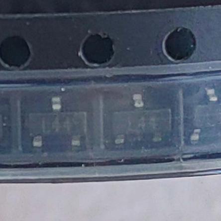
Image for reference only

制造商零件:

BAT54SW

包装:

SOT-323 / SC-70(2.0 x 1.25 x 0.95 毫米,3 引线)

品牌:
产品类别:
您可能感兴趣的其他建议.
说明

The BAT54SW from Nexperia is a series-pair Schottky barrier diode in a compact SOT-323 (SC-70) surface-mount package (2.0 x 1.25 x 0.95 mm). The series configuration connects two diodes in series (anode of D1 to cathode of D2), providing higher reverse voltage blocking in a single package. Key specifications: VRRM = 30V, IF = 200mA continuous (300mA per ST version), forward voltage VF = 240mV max at IF=0.1mA, 320mV max at IF=1mA, 400mV max at IF=10mA, total capacitance CT = 10pF max at VR=1V/f=1MHz, reverse leakage IR = 2uA max at VR=25V, reverse recovery time trr = 5ns. Planar Schottky barrier construction with integrated guard ring for stress protection. Junction temperature: -55C to 150C (Nexperia) or 125C (some manufacturers). Power dissipation: 200mW (SOT-323). Active product, RoHS compliant, marking code L44/44%.

The BAT54SW from Nexperia is a series-pair Schottky barrier diode housed in a compact SOT-323 (SC-70) surface-mount plastic package. The BAT54 family offers multiple diode configurations in the same small footprint, with the suffix letter indicating the topology: no letter or W = single diode, A = common anode pair, C = common cathode pair, and S = series pair. The BAT54SW specifically contains two Schottky diodes connected in series (anode of D1 connected to cathode of D2 internally), providing double the reverse voltage blocking capability in a single package compared to a single diode.

Schottky barrier diodes are fundamentally different from conventional PN junction diodes. They use a metal-semiconductor (Schottky) junction rather than a semiconductor-semiconductor (PN) junction, resulting in several key advantages: (1) Much lower forward voltage drop (typically 240-400mV vs 600-700mV for silicon PN diodes at low currents), which reduces conduction losses and improves efficiency; (2) Extremely fast switching speed with negligible reverse recovery time (5ns vs 25-50ns for small-signal PN diodes), because Schottky diodes are majority-carrier devices with no stored minority charge to remove during turn-off; (3) Low junction capacitance (10pF max), making them suitable for high-frequency applications.

The series configuration of the BAT54SW means the effective forward voltage drop is approximately double that of a single Schottky diode (two diode drops in series), but the reverse blocking capability is also doubled. At low currents (IF=1mA), the total forward drop is approximately 640mV (2 x 320mV), still competitive with a single silicon PN diode (600-700mV) while providing the fast switching and low capacitance benefits of Schottky technology. At higher currents, the advantage is less pronounced because two Schottky drops can exceed a single PN drop.

The SOT-323 (SC-70) package is approximately 50% smaller than the more common SOT-23 package, making it ideal for space-constrained applications such as mobile phones, tablets, and other portable electronics. The package has a footprint of only 2.0 x 1.25 mm with a height of 0.95 mm. The trade-off is lower power dissipation (200mW vs 250-350mW for SOT-23) due to the smaller thermal mass and reduced PCB heat spreading area.

The planar Schottky barrier construction uses a metal-silicon junction formed by depositing a metal layer (typically platinum, titanium, or molybdenum) on a lightly doped N-type silicon epitaxial layer. The integrated guard ring is a P-type diffusion surrounding the Schottky contact that serves as a protection against excessive reverse voltage stress. The guard ring acts as a conventional PN junction that begins to conduct under reverse bias conditions, distributing the electric field and preventing localized breakdown at the edges of the Schottky contact.

The BAT54SW is widely used in applications requiring low forward voltage drop, fast switching, and compact size. Common uses include voltage clamping, reverse polarity protection, logic level translation, RF signal routing, and power supply ORing. The series configuration is particularly useful when a higher reverse voltage rating is needed than a single diode can provide, or when the voltage drop across two diodes is actually desired (e.g., creating a reference voltage of approximately 0.6V from a supply rail).

The BAT54SW operates as a series-pair Schottky barrier diode using metal-semiconductor junctions.

Schottky Barrier Junction: Unlike a conventional PN junction diode where both P-type and N-type semiconductors form the junction, a Schottky diode uses a metal-semiconductor junction. When a metal with a suitable work function (typically platinum, titanium-silicide, or chromium) is brought into contact with N-type silicon, a potential barrier (the Schottky barrier) forms at the interface. The height of this barrier depends on the metal work function and the semiconductor doping, and is typically 0.3-0.5V for the metals used in BAT54 series diodes, compared to 0.6-0.7V for a silicon PN junction.

Forward Bias Operation: When a positive voltage is applied to the anode (metal) relative to the cathode (N-type silicon), the barrier height is reduced, allowing electrons to flow from the N-type silicon into the metal. Because the conduction mechanism is primarily thermionic emission of majority carriers (electrons) over the barrier, there is no minority carrier injection and no stored charge in the drift region. This results in the characteristic low forward voltage drop and fast switching of Schottky diodes. The forward current increases exponentially with applied voltage, following the thermionic emission model: IF = IS x (exp(VF/nVT) – 1), where IS is the saturation current, n is the ideality factor (typically 1.0-1.1 for Schottky diodes, close to ideal), and VT is the thermal voltage (26mV at 25C).

Reverse Bias Operation: When a negative voltage is applied to the anode relative to the cathode, the barrier height increases, blocking current flow. However, a small reverse leakage current flows due to thermionic emission of electrons over the barrier in the reverse direction. This reverse current increases exponentially with temperature, approximately doubling for every 10C rise. At 25C, the reverse leakage is typically 1-2uA at VR=25V, but can increase to 100uA or more at 100C. This temperature-dependent leakage is the primary disadvantage of Schottky diodes compared to PN diodes.

Series Configuration: In the BAT54SW, two Schottky diodes are connected in series internally: the cathode of D1 is connected to the anode of D2. When forward current flows from Pin 1 (anode of D1) through Pin 3 (cathode of D2), it passes through both diodes sequentially, and the total forward voltage drop is the sum of the two individual diode drops. In reverse bias, the reverse voltage is shared between the two diodes (assuming matched characteristics), effectively doubling the reverse voltage capability. The common connection point between the two diodes is brought out to Pin 2, which can be used for various circuit configurations.

Guard Ring Protection: The integrated P-type guard ring surrounding the Schottky contact serves as a voltage stress protection mechanism. Under normal forward or low reverse bias conditions, the guard ring is inactive and the Schottky junction dominates the device behavior. Under high reverse bias, the electric field at the edge of the Schottky contact can become very concentrated, potentially causing localized avalanche breakdown and device damage. The guard ring PN junction begins to conduct under these conditions, spreading the electric field more uniformly and raising the effective breakdown voltage. This allows the BAT54SW to reliably block 30V despite the relatively low Schottky barrier height.

Capacitance and Switching: The total capacitance of the Schottky diode consists of the junction capacitance (depletion capacitance) and the package parasitic capacitance. The junction capacitance is voltage-dependent (decreasing with increasing reverse bias) and is specified as 10pF max at VR=1V. The reverse recovery time of 5ns is primarily limited by the RC time constant of the junction capacitance and the circuit resistance, not by stored charge recombination (as in PN diodes). This makes Schottky diodes virtually free of reverse recovery losses, a critical advantage in high-frequency switching applications.

针脚 名称 类型 说明
1 Anode 1 阳极 Anode of diode D1; current enters the device through this pin in the forward direction; connects internally to the Schottky metal contact of D1
2 Common (D1 Cathode / D2 Anode) 输入/输出 Internal connection point between cathode of D1 and anode of D2; can be left floating in simple series configuration or connected to a reference voltage for specific circuit topologies
3 Cathode 2 阴极 Cathode of diode D2; current exits the device through this pin in the forward direction; connects internally to the N-type silicon of D2
应用 说明
Voltage Clamping Use series pair to clamp signal lines to a defined voltage range; two diode drops provide approximately 0.5-0.7V clamp window; useful for protecting microcontroller inputs from moderate overvoltage; fast response time (5ns trr) handles transient events effectively
Reverse Polarity Protection Series configuration blocks reverse voltage up to 30V; very low forward drop (approximately 0.5V total at moderate current) minimizes voltage loss compared to PN diode protection; compact SOT-323 package fits space-constrained designs
逻辑电平转换 Create voltage level shifts using the known forward voltage drop; two series Schottky drops provide approximately 0.5-0.7V shift; useful for translating between 3.3V and 2.5V or similar closely-spaced logic levels; fast switching preserves signal integrity
RF Signal Steering Low capacitance (10pF) and fast switching (5ns) make BAT54SW suitable for RF signal routing and antenna switching applications; Schottky diodes are preferred over PN diodes in RF circuits due to lower noise and faster response; series pair provides better isolation in reverse bias
Power Supply ORing Combine two power sources using the series diode drops to prevent back-feeding between supplies; low forward drop minimizes power loss; common pin (Pin 2) can be connected to a pull-up or pull-down for specific ORing configurations
模型 制造商 兼容性 主要区别
BAT54S Nexperia/ST Same Config, Larger Package Series-pair Schottky in SOT-23 package; identical electrical characteristics; larger package (2.9 x 1.3mm vs 2.0 x 1.25mm); higher power dissipation (250-350mW vs 200mW); use when PCB space is not critical
BAT54CW Nexperia Common Cathode Variant Common cathode pair in SOT-323; two cathodes connected together; different circuit topology; same electrical characteristics per diode; use when common-cathode configuration is needed
BAT54AW Nexperia Common Anode Variant Common anode pair in SOT-323; two anodes connected together; different circuit topology; same electrical characteristics per diode; use when common-anode configuration is needed
BAT54W Nexperia Single Diode Variant Single Schottky diode in SOT-323; lower forward drop (single diode); use when series configuration is not needed; same package and overall dimensions
1N5817 各种 Through-Hole Schottky 1A, 20V Schottky diode in DO-41 axial package; much higher current rating; through-hole mounting; larger footprint; for power rectification rather than signal applications
推荐部件
SPDT analog switch, 6Ω RON, 1.65-5.5V, 300MHz BW, BBM, TSSOP6

品牌:

封装:

TSSOP6 / SOT363-2 (2.1 x 1.25 x 0.95mm)
有库存:
14113pcs

货运周期:3~7 天
最低订购量为 1

转到查询
双共阴极肖特基、30V、200mA、240mV@1mA、5ns trr、SOT-23、AEC-Q101

品牌:

封装:

SOT-23 / TO-236AB(2.9 x 1.3 x 1.0 毫米,1.9 毫米间距)
有库存:
362417 件

货运周期:3~7 天
最低订购量为 1

转到查询
PNP 40V 200mA、hFE 100-300、fT 250MHz、SOT-23、与 MMBT3904 互补、通用开关器件

品牌:

封装:

SOT-23 (TO-236)(2.9 x 1.3 x 1.0 毫米,1.9 毫米间距)
有库存:
80000 件

货运周期:3~7 天
最低订购量为 1

转到查询
N 沟道小信号 MOSFET,50V/173mA,15 欧姆 RDS(on)@10V,逻辑电平,TrenchMOS,SOT-23,-65~150C

品牌:

封装:

SOT-23 (TO-236AB)(2.9 x 1.3 x 1.0 毫米,1.9 毫米间距)
有库存:
0 件

货运周期:3~7 天
最低订购量为 1

转到查询
八进制总线收发器,3 态,非反相,TTL 输入,4.5-5.5V,10ns prop 延迟,TSSOP-20,-40~125C

品牌:

封装:

TSSOP-20 (SOT360-1)(6.50 x 6.40 x 1.10 毫米,0.65 毫米间距)
有库存:
550000 件

货运周期:3~7 天
最低订购量为 1

转到查询
八位 D 型透明锁存器,3 态输出,LE 和 OE 控制,2-6V,TSSOP-20,-40~125C,I/O 位于总线接口的对侧

品牌:

封装:

TSSOP-20 (SOT360-1) (6.4 x 4.4 x 1.2 mm)
有库存:
24829 件

货运周期:3~7 天
最低订购量为 1

转到查询
质量保证

我们从合作供应链采购的所有电子元件都经过严格的进货检验。通过仔细的测试,我们确保交付给客户的所有产品都是原装正品,符合质量要求。此外,我们还保存完整的检验记录,使整个供应链流程清晰可查。.

认证
我们获得了多项专业认证,并建立了自己的专业检测实验室,确保交付给客户的每一件产品都符合最高质量要求。我们严格按照流程进行检测,确保产品质量稳定、参数准确。为保证原装正品,我们还与可靠的第三方检测机构合作,进行严格的质量检测。我们始终高度重视质量,完全符合行业标准、相关法规和 ISO 9001:2015 的要求。.

发货与付款

我们从合作供应链采购的所有电子元件都经过严格的进货检验。通过仔细的测试,我们确保交付给客户的所有产品都是原装正品,符合质量要求。此外,我们还保存完整的检验记录,使整个供应链流程清晰可查。.

认证
我们获得了多项专业认证,并建立了自己的专业检测实验室,确保交付给客户的每一件产品都符合最高质量要求。我们严格按照流程进行检测,确保产品质量稳定、参数准确。为保证原装正品,我们还与可靠的第三方检测机构合作,进行严格的质量检测。我们始终高度重视质量,完全符合行业标准、相关法规和 ISO 9001:2015 的要求。.

服务与包装

我们从合作供应链采购的所有电子元件都经过严格的进货检验。通过仔细的测试,我们确保交付给客户的所有产品都是原装正品,符合质量要求。此外,我们还保存完整的检验记录,使整个供应链流程清晰可查。.

认证
我们获得了多项专业认证,并建立了自己的专业检测实验室,确保交付给客户的每一件产品都符合最高质量要求。我们严格按照流程进行检测,确保产品质量稳定、参数准确。为保证原装正品,我们还与可靠的第三方检测机构合作,进行严格的质量检测。我们始终高度重视质量,完全符合行业标准、相关法规和 ISO 9001:2015 的要求。.



