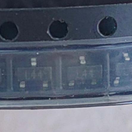
The BAT54SW operates as a series-pair Schottky barrier diode using metal-semiconductor junctions.
Schottky Barrier Junction: Unlike a conventional PN junction diode where both P-type and N-type semiconductors form the junction, a Schottky diode uses a metal-semiconductor junction. When a metal with a suitable work function (typically platinum, titanium-silicide, or chromium) is brought into contact with N-type silicon, a potential barrier (the Schottky barrier) forms at the interface. The height of this barrier depends on the metal work function and the semiconductor doping, and is typically 0.3-0.5V for the metals used in BAT54 series diodes, compared to 0.6-0.7V for a silicon PN junction.
Forward Bias Operation: When a positive voltage is applied to the anode (metal) relative to the cathode (N-type silicon), the barrier height is reduced, allowing electrons to flow from the N-type silicon into the metal. Because the conduction mechanism is primarily thermionic emission of majority carriers (electrons) over the barrier, there is no minority carrier injection and no stored charge in the drift region. This results in the characteristic low forward voltage drop and fast switching of Schottky diodes. The forward current increases exponentially with applied voltage, following the thermionic emission model: IF = IS x (exp(VF/nVT) – 1), where IS is the saturation current, n is the ideality factor (typically 1.0-1.1 for Schottky diodes, close to ideal), and VT is the thermal voltage (26mV at 25C).
Reverse Bias Operation: When a negative voltage is applied to the anode relative to the cathode, the barrier height increases, blocking current flow. However, a small reverse leakage current flows due to thermionic emission of electrons over the barrier in the reverse direction. This reverse current increases exponentially with temperature, approximately doubling for every 10C rise. At 25C, the reverse leakage is typically 1-2uA at VR=25V, but can increase to 100uA or more at 100C. This temperature-dependent leakage is the primary disadvantage of Schottky diodes compared to PN diodes.
Series Configuration: In the BAT54SW, two Schottky diodes are connected in series internally: the cathode of D1 is connected to the anode of D2. When forward current flows from Pin 1 (anode of D1) through Pin 3 (cathode of D2), it passes through both diodes sequentially, and the total forward voltage drop is the sum of the two individual diode drops. In reverse bias, the reverse voltage is shared between the two diodes (assuming matched characteristics), effectively doubling the reverse voltage capability. The common connection point between the two diodes is brought out to Pin 2, which can be used for various circuit configurations.
Guard Ring Protection: The integrated P-type guard ring surrounding the Schottky contact serves as a voltage stress protection mechanism. Under normal forward or low reverse bias conditions, the guard ring is inactive and the Schottky junction dominates the device behavior. Under high reverse bias, the electric field at the edge of the Schottky contact can become very concentrated, potentially causing localized avalanche breakdown and device damage. The guard ring PN junction begins to conduct under these conditions, spreading the electric field more uniformly and raising the effective breakdown voltage. This allows the BAT54SW to reliably block 30V despite the relatively low Schottky barrier height.
Capacitance and Switching: The total capacitance of the Schottky diode consists of the junction capacitance (depletion capacitance) and the package parasitic capacitance. The junction capacitance is voltage-dependent (decreasing with increasing reverse bias) and is specified as 10pF max at VR=1V. The reverse recovery time of 5ns is primarily limited by the RC time constant of the junction capacitance and the circuit resistance, not by stored charge recombination (as in PN diodes). This makes Schottky diodes virtually free of reverse recovery losses, a critical advantage in high-frequency switching applications.





 English
  简体中文
简体中文  Español
  العربية




