Home > Integrated Circuits ICs > STMPS2171STR

STMPS2171STR


1A high-side power switch, 90mOhm N-MOSFET, UVLO, OCP, OTP, fault blanking, reverse current block, SOT-23-5, 2.7-5.5V, -40~85C

20000

Effective Inventory
Go to Inquiry

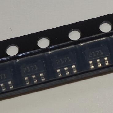
Image for reference only

Manufacturer Part:

STMPS2171STR

Package:

SOT-23-5 (SC-74A / SOT-753) (3.0 x 1.75 x 1.3 mm, 0.95mm pitch)

Brand:
Product Categories:
Other recommendations you may be interested in.
Description

The STMPS2171STR from STMicroelectronics is a single-channel high-side power distribution switch with a 90 mOhm N-channel MOSFET in a 5-pin SOT-23 package with tape and reel packaging. Key specifications: 1 A continuous output current; 90 mOhm typical RDS(on) N-channel MOSFET switch (120 mOhm maximum); operating input voltage range 2.7 V to 5.5 V; output voltage range 0 to 5.5 V; CMOS and TTL compatible enable (EN) input; active-high enable (switch on when EN is HIGH); undervoltage lockout (UVLO) turns switch off when input drops below threshold; overcurrent protection with constant current limiting at approximately 120 percent of rated current; thermal shutdown at junction temperature approximately 135 degrees C with 10 degree hysteresis; reverse current blocking when switch is OFF or unpowered; fault-blanking (10 ms typical) prevents false fault signals during hot-swap capacitive load inrush; open-drain FAULT output (active-low) indicates overcurrent or thermal fault; 12 uA maximum standby supply current when disabled; 8 kV ESD protection (HBM); UL recognized component (UL file E354278); operating temperature -40 to +85 degrees C (ambient) or -40 to +125 degrees C (junction); thermal resistance SOT-23-5: 191 degrees C/W. The STMPS2171 is the 1 A variant; the family also includes STMPS2141 (0.5 A), STMPS2151 (0.5 A with different current limit), and STMPS2161 (1 A with different current limit). MSL Level-1-260C-UNLIM. EcoPack3 (RoHS compliant). Active/Production status.

The STMPS2171STR from STMicroelectronics is a single-channel high-side power distribution switch designed for applications where heavy capacitive loads and short circuits are likely to be encountered, such as USB port power distribution, hot-swap power supplies, and general-purpose load switching.

The STMPS2171 integrates a 90 mOhm N-channel MOSFET power switch with comprehensive protection features (overcurrent, thermal shutdown, undervoltage lockout, reverse current blocking) and a fault reporting output, all in a tiny 5-pin SOT-23 package. This level of integration replaces what would otherwise require a discrete MOSFET, gate driver, current sense resistor, comparator, and thermal protection circuit, reducing component count, PCB area, and design complexity.

The STMPS2171 is the 1 A continuous current variant in the STMPS21x1 family. The family includes four members with different current ratings: STMPS2141 (0.5 A), STMPS2151 (0.5 A, different current limit threshold), STMPS2161 (1 A, different current limit threshold), and STMPS2171 (1 A). All share the same pinout and package, allowing different current limit options without PCB changes.

The N-channel MOSFET switch provides 90 mOhm typical on-resistance (120 mOhm maximum), which results in only 90 mV of voltage drop at 1 A load current. This low voltage drop ensures that the load receives nearly the full input voltage, which is critical for USB applications where the voltage at the device must remain above 4.75 V (USB 2.0 specification minimum) from a 5 V source.

The high-side switch topology means the switch is placed between the power supply and the load (in the positive rail), rather than in the ground return path. This is the preferred topology for USB and hot-swap applications because it completely disconnects the load from the supply when the switch is off, preventing any sneak current paths. The N-channel MOSFET is used with an internal charge pump to generate the gate voltage above the input voltage, ensuring the MOSFET can be fully enhanced even when VIN equals VOUT.

The overcurrent protection limits the output current to approximately 120 percent of the rated current (approximately 1.2 A for the STMPS2171) when a fault occurs. The constant-current limiting mode prevents the MOSFET from being damaged by excessive current, while the thermal shutdown provides a secondary protection layer if the current limit condition persists and the junction temperature rises above 135 degrees C.

The 10 ms fault-blanking feature is particularly important for hot-swap applications. When a load with large input capacitors is connected to the output, the inrush current can momentarily exceed the current limit threshold. Without fault blanking, this would cause a false FAULT assertion and potentially shut down the port. The 10 ms blanking period allows the capacitive inrush current to settle before the FAULT output is asserted, preventing nuisance fault signals during normal hot-swap events.

The reverse current blocking feature prevents current from flowing backward from the output to the input when the switch is disabled (EN = LOW) or when the device is unpowered (VIN = 0 V). This is important in battery-powered applications where the battery may be disconnected while the output is still connected to a powered external device, or in multi-source systems where one supply may backfeed through the switch.

The UL recognition (file E354278) is important for equipment that must meet UL safety standards, as it simplifies the certification process for the overall system.

At $0.32 per unit in volume (1000+), the STMPS2171STR is one of the most cost-effective 1 A high-side power switches available, making it practical to add protection and switching to every USB port and power rail in a system.

The STMPS2171STR operates as a high-side N-channel MOSFET power switch with integrated charge pump, current limiting, thermal protection, and fault reporting.

N-Channel MOSFET Switch: The power switching element is an N-channel MOSFET connected between the VIN and VOUT pins. To fully enhance an N-channel MOSFET (turn it on with minimum RDS(on)), the gate voltage must be higher than the source voltage by at least the threshold voltage (VGS(th), typically 1-2 V) plus the desired overdrive. Since the source is connected to VIN, the gate must be driven above VIN. An internal charge pump generates this gate drive voltage from the input supply. The charge pump operates continuously when the switch is enabled, maintaining the gate voltage approximately 5 V above VIN to ensure the MOSFET is fully enhanced. When the switch is disabled (EN = LOW) or during UVLO, the charge pump stops and the gate is pulled to ground, turning off the MOSFET.

Enable Control: The EN pin is a logic input with CMOS and TTL compatible thresholds. When EN is HIGH (above approximately 1.5 V), the charge pump operates and the MOSFET is turned on. When EN is LOW (below approximately 0.8 V), the charge pump stops and the MOSFET is turned off. The enable input can be driven directly by a microcontroller GPIO or by logic circuits. The standby current when disabled is only 12 uA maximum.

Undervoltage Lockout (UVLO): The UVLO circuit monitors the input voltage (VIN). When VIN drops below the UVLO threshold (approximately 2.0-2.5 V), the switch is forced off regardless of the EN input state. This prevents the MOSFET from operating with insufficient gate drive voltage, which could cause it to operate in the linear region with high RDS(on) and excessive power dissipation. The UVLO has hysteresis (approximately 100-200 mV) to prevent chattering near the threshold. The FAULT output is asserted immediately when UVLO activates.

Current Limiting: The current limiting circuit monitors the current through the MOSFET using an internal sense element (a scaled replica of the power MOSFET). When the output current exceeds the current limit threshold (approximately 1.2 A for the STMPS2171), the circuit reduces the gate drive voltage to limit the current to the threshold value. The MOSFET operates in the constant-current mode, maintaining the current at the limit value while the output voltage drops. If the current limit condition persists and the MOSFET power dissipation (VIN – VOUT) x ILIMIT causes the junction temperature to rise above 135 degrees C, the thermal shutdown activates.

Thermal Shutdown: The thermal sensor on the die monitors the junction temperature. When the junction temperature exceeds approximately 135 degrees C, the MOSFET is turned off completely to prevent damage. The FAULT output is asserted immediately (no blanking). When the junction temperature drops below approximately 125 degrees C (10 degree hysteresis), the switch automatically restarts with the current limit active, allowing it to safely drive the load again if the fault has been cleared.

Fault Blanking: The 10 ms fault blanking timer prevents false FAULT assertions during transient events. When the output current exceeds the current limit, an internal counter starts. The FAULT output is not asserted until the counter reaches the 10 ms timeout. If the overcurrent condition clears before 10 ms (e.g., capacitive inrush current that decays quickly), the FAULT output is never asserted. Only current limit faults are blanked; thermal shutdown and UVLO faults assert FAULT immediately without blanking.

Reverse Current Blocking: When the switch is OFF (EN = LOW or UVLO active), the body diode of the N-channel MOSFET would normally conduct current from VOUT to VIN (reverse direction). The STMPS2171 includes a circuit that disconnects the body diode path when the switch is off, preventing any reverse current flow. When the device is unpowered (VIN = 0 V), the switch presents a high impedance at the output pin.

FAULT Output: The FAULT pin is an open-drain N-channel MOSFET output that pulls LOW when a fault is detected. The FAULT output is asserted in the following conditions: overcurrent (after 10 ms blanking), thermal shutdown (immediate), and UVLO (immediate). The FAULT output can be wire-ORed with other FAULT outputs from additional power switches, creating a single fault signal for the system. An external pull-up resistor (10-100 kOhm) is required.

Pin Name Type Description
1 OUT Power Output Switch output; connects to the load; voltage range 0 to 5.5 V; up to 1 A continuous current; the N-channel MOSFET connects VIN to OUT when enabled; when disabled, OUT is high impedance (reverse current blocked); connect output capacitor (0.1-1 uF) to GND for stability; larger capacitors (10-100 uF) at the load are acceptable and are protected by the current limit and fault blanking during hot-swap
2 GND Ground Ground reference; connect to PCB ground plane; provides the ground reference for the internal control circuitry and the source terminal of the current sense element; the GND pin must carry the full load current return path; keep the GND trace short and wide; bypass VIN to GND with a 0.1 uF ceramic capacitor near the pin
3 EN Input Enable input; active-high; CMOS and TTL compatible logic threshold; pull HIGH (above 1.5 V) to turn on the switch; pull LOW (below 0.8 V) to turn off the switch and enter standby mode (12 uA max); do not leave floating; connect to VIN through a 100 kOhm pull-up for always-on operation; can be driven by MCU GPIO for controlled switching; EN voltage range extends to 6 V (independent of VIN)
4 FAULT Output Fault indicator output; open-drain N-channel MOSFET (active-low); pulls LOW when a fault is detected (overcurrent after blanking, thermal shutdown, or UVLO); high impedance when no fault; requires an external pull-up resistor (10-100 kOhm) to a logic supply; can be wire-ORed with other FAULT outputs; the FAULT output does not indicate the type of fault; the MCU must determine the fault type by reading the EN state and measuring VIN and VOUT
5 IN Power Input Power supply input; 2.7 V to 5.5 V; connects to the drain of the N-channel MOSFET; bypass with a 0.1 uF ceramic capacitor to GND placed close to the pin; a 1-10 uF bulk capacitor on the input supply is recommended; the input voltage must be above the UVLO threshold for the switch to operate; the charge pump draws power from this pin to generate the gate drive voltage
Application Description
USB Port Power Switch Protect USB ports from overcurrent and short-circuit faults; 90 mOhm RDS(on) drops only 90 mV at 1 A, keeping voltage within USB spec (4.75 V min at device); fault blanking accommodates capacitive inrush during device connection; FAULT output signals host controller; EN pin allows host to disable port; UL recognized for USB equipment certification; 8 kV ESD protects against cable discharge events
Hot-Swap Power Supply Enable safe insertion and removal of circuit boards or modules into a live backplane; current limit prevents supply droop during board insertion; fault blanking ignores capacitive inrush; thermal shutdown protects against sustained overloads; reverse current blocking prevents backfeed when board is removed; EN pin controls power-up sequence after board is seated
Motor / Solenoid Driver Protection Switch and protect low-power motor or solenoid circuits; 1 A current limit handles most small DC motors; thermal shutdown protects against stalled motor condition; FAULT output alerts system to stall; EN pin provides on/off control from MCU; add flyback diode across inductive loads; SOT-23-5 package fits near the motor connector
LED String Power Switch Switch power to LED strings or LED modules; 1 A handles multiple high-brightness LEDs; current limit protects against wiring faults; thermal shutdown prevents overheating; EN pin enables PWM dimming when driven by MCU PWM output (up to a few kHz); very low standby current (12 uA) when LEDs are off
Battery-Powered Load Switch Disconnect loads from battery to extend shelf life; 12 uA standby current has minimal impact on battery; reverse current blocking prevents battery discharge through disabled loads; UVLO prevents operation below minimum battery voltage; FAULT output signals low battery or overload condition; simple EN control from MCU or pushbutton
Model Manufacturer Compatibility Key Difference
STMPS2161STR STMicroelectronics Same Family, Different Current Limit Same STMPS21x1 family; 1 A rated current; different current limit threshold (higher or lower depending on variant); same SOT-23-5 pinout; same protection features; use as drop-in alternative when a different current limit threshold is needed for the application; verify current limit specification for the specific variant
STMPS2141STR STMicroelectronics Same Family, Lower Current 0.5 A rated current version; same SOT-23-5 pinout; lower current limit threshold; lower RDS(on) (same 90 mOhm typical); use when 0.5 A is sufficient; lower cost in some cases; same protection features
TPS2041BDBVR TI Functional Equivalent 1 A high-side power switch; SOT-23-5; 70 mOhm RDS(on) (lower); similar UVLO, OCP, thermal shutdown; open-drain OC output; different pinout (not pin-compatible); use as alternative source; verify pin assignments before PCB layout
AP2141SG-13 Diodes Inc Functional Equivalent 1 A high-side power switch; SOT-23-5; similar specifications; same pinout as TPS2041 (different from STMPS2171); lower cost; use as alternative source; verify pinout compatibility
FDC6325L onsemi Discrete MOSFET Alternative Dual N/P-channel MOSFET in SOT-23-6; not an integrated power switch; requires external gate drive and protection; lower cost per switch but higher component count; no current limit, no thermal protection, no fault output; use when a simple load switch is sufficient and protection features are implemented in firmware
Recommend Parts
Cortex-M0+ ultra-low-power MCU, 32MHz, 128KB Flash, crystal-less USB, LQFP-64

Brand:

Package:

LQFP-64 (10×10 mm)
In stock:
14446pcs

Cargo cycle: 3~7 Days
The minimum order is 1

Go to Inquiry
Cortex-M4F MCU, 168MHz, 512KB Flash, 192KB SRAM, Ethernet, USB OTG, LQFP-100

Brand:

Package:

LQFP-100 (14×14×1.4 mm)
In stock:
2870pcs

Cargo cycle: 3~7 Days
The minimum order is 1

Go to Inquiry
ARM Cortex-M4F MCU, 72MHz, 384KB Flash, 64KB SRAM, dual ADC, 4 comparators, 2 op amps, LQFP-100

Brand:

Package:

LQFP-100 (14 x 14 x 1.4 mm)
In stock:
12274pcs

Cargo cycle: 3~7 Days
The minimum order is 1

Go to Inquiry
ARM Cortex-M4F MCU, 168MHz, 1MB Flash, 192KB SRAM, Ethernet, USB OTG HS, UFBGA-176

Brand:

Package:

UFBGA-176 (10 x 10 mm, 0.65mm pitch)
In stock:
9303pcs

Cargo cycle: 3~7 Days
The minimum order is 1

Go to Inquiry
Quad JFET-input op amp, 4MHz GBP, 16V/µs slew rate, 200pA bias current, SOIC-14

Brand:

Package:

SOIC-14 (8.75 x 4 x 1.65 mm)
In stock:
9834pcs

Cargo cycle: 3~7 Days
The minimum order is 1

Go to Inquiry
Ultra-low-power Cortex-M3 MCU, 32MHz, 256KB Flash, 32KB SRAM, LCD controller, LQFP-64

Brand:

Package:

LQFP-64 (10x10mm)
In stock:
5417pcs

Cargo cycle: 3~7 Days
The minimum order is 1

Go to Inquiry
Quality Assurance

All electronic components we source from our partnered supply chains go through strict incoming inspections.Through careful testing, we ensure everything delivered to customers is genuine original parts and meets quality requirements.In addition, we keep complete inspection records to make the entire supply chain process clear and traceable.

Certification
We have obtained a number of professional certifications and built our own professional testing laboratory.This ensures that every product we deliver to our customers meets the highest quality requirements.We conduct tests in strict accordance with procedures to ensure stable product quality and accurate parameters.To guarantee genuine original parts, we also cooperate with reliable third-party testing institutions for strict quality inspection.We always attach great importance to quality and fully comply with industry standards, relevant regulations, and ISO 9001:2015 requirements.

Shipping & Payment

All electronic components we source from our partnered supply chains go through strict incoming inspections.Through careful testing, we ensure everything delivered to customers is genuine original parts and meets quality requirements.In addition, we keep complete inspection records to make the entire supply chain process clear and traceable.

Certification
We have obtained a number of professional certifications and built our own professional testing laboratory.This ensures that every product we deliver to our customers meets the highest quality requirements.We conduct tests in strict accordance with procedures to ensure stable product quality and accurate parameters.To guarantee genuine original parts, we also cooperate with reliable third-party testing institutions for strict quality inspection.We always attach great importance to quality and fully comply with industry standards, relevant regulations, and ISO 9001:2015 requirements.

Service & Packaging

All electronic components we source from our partnered supply chains go through strict incoming inspections.Through careful testing, we ensure everything delivered to customers is genuine original parts and meets quality requirements.In addition, we keep complete inspection records to make the entire supply chain process clear and traceable.

Certification
We have obtained a number of professional certifications and built our own professional testing laboratory.This ensures that every product we deliver to our customers meets the highest quality requirements.We conduct tests in strict accordance with procedures to ensure stable product quality and accurate parameters.To guarantee genuine original parts, we also cooperate with reliable third-party testing institutions for strict quality inspection.We always attach great importance to quality and fully comply with industry standards, relevant regulations, and ISO 9001:2015 requirements.









