Home > Integrated Circuits ICs > SN74LVC8T245PWR

SN74LVC8T245PWR


8-bit dual-supply bus transceiver, 1.65-5.5V configurable level shifter, TSSOP-24, 200Mbps

5569

Effective Inventory
Go to Inquiry

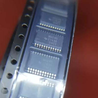
Image for reference only

Manufacturer Part:

SN74LVC8T245PWR

Package:

TSSOP-24 (7.8 x 4.4 mm)

Brand:
Product Categories:
Other recommendations you may be interested in.
Description

The SN74LVC8T245PWR is an 8-bit dual-supply bus transceiver with configurable voltage-level shifting and three-state outputs from Texas Instruments in a TSSOP-24 (7.8 x 4.4 mm) package. It features independent VCCA and VCCB supply rails (1.65V-5.5V each) enabling bidirectional translation between any two voltage nodes. Key specs: 200 Mbps max data rate, 6.6 ns typical propagation delay, ±32 mA output drive, three-state outputs controlled by DIR and OE pins. VCC isolation and Ioff circuitry support partial-power-down and hot-swap applications. ESD protection: 4000V HBM, 100V MM, 1000V CDM. Latch-up exceeds 100 mA (JESD 78 Class II). Tape and reel packaging (2000/reel). Operating temperature: -40°C to +85°C. Ideal for SPI, UART, I2S, JTAG, GPIO level shifting in multi-voltage embedded systems.

The SN74LVC8T245PWR is an 8-bit dual-supply bus transceiver with configurable voltage-level shifting and three-state outputs, manufactured by Texas Instruments. It belongs to the 74LVC family of low-voltage CMOS logic devices and is designed for bidirectional voltage-level translation between two independently powered data buses.

The device features two independent supply rails: VCCA (1.65V to 5.5V) for the A port and VCCB (1.65V to 5.5V) for the B port. This fully configurable dual-rail architecture allows translation between any two voltage nodes in the 1.65V to 5.5V range, including common combinations such as 1.8V to 3.3V, 2.5V to 3.3V, 3.3V to 5V, and any other valid pairing. The direction of data flow is controlled by the DIR (direction) input pin, and the outputs can be placed in a high-impedance state using the OE (output enable, active-low) input pin.

The SN74LVC8T245 supports a maximum data rate of 200 Mbps, making it suitable for high-speed digital interfaces including SPI, UART, I2S, JTAG, GPIO, and PCM. The propagation delay is typically 6.6 ns. The device provides ±32 mA output drive current on both ports, ensuring robust signal integrity across a wide range of load conditions.

A key feature is the VCC isolation function: when either VCCA or VCCB is grounded, all outputs are placed in the high-impedance state, preventing back-drive current from the active supply rail into the disabled side. The Ioff circuitry supports partial-power-down operation, ensuring that no destructive current flows back through the device when one or both supply rails are de-energized. This makes the SN74LVC8T245 suitable for hot-swap and live-insertion applications.

The device provides excellent ESD protection: 4000V HBM (Human Body Model), 100V MM (Machine Model), and 1000V CDM (Charged Device Model). Latch-up performance exceeds 100 mA per JESD 78 Class II. The control inputs (DIR and OE) reference VCCA for their VIH/VIL thresholds.

The PWR suffix denotes the TSSOP-24 (PW) package with tape and reel packaging (2,000 units per reel). The TSSOP-24 package measures 7.8 × 4.4 mm with a maximum height of 1.05 mm, making it suitable for space-constrained PCB layouts. Operating temperature range is -40°C to +85°C.

The SN74LVC8T245PWR operates as an 8-bit non-inverting bidirectional bus transceiver with configurable voltage-level translation between two independently powered bus domains.

Dual-Supply Architecture: The device has two independent power supply rails: VCCA powers the A port (pins A1-A8) and VCCB powers the B port (pins B1-B8). Each supply can be set independently within the 1.65V to 5.5V range. The A port I/O pins have input thresholds and output levels referenced to VCCA, while the B port I/O pins are referenced to VCCB. This dual-rail design is the fundamental mechanism that enables voltage-level translation: when data passes from the A port to the B port (or vice versa), the input signal is received at one voltage domain and the output is driven at the other voltage domain.

Direction Control (DIR): The DIR pin determines the direction of data flow between the A and B ports. When DIR is HIGH (referenced to VCCA thresholds), data flows from the A port to the B port: A1-A8 are configured as inputs, and B1-B8 are configured as outputs that follow the A port logic levels translated to the VCCB domain. When DIR is LOW, the direction reverses: B1-B8 become inputs and A1-A8 become outputs translated to the VCCA domain. This direction control is a global setting that applies to all 8 bits simultaneously; the SN74LVC8T245 does not support bit-wise independent direction control.

Output Enable (OE): The OE pin is an active-low output enable referenced to VCCA logic thresholds. When OE is LOW, the transceiver is active and data flows according to the DIR setting. When OE is HIGH, all outputs (both A port and B port) are placed in the high-impedance (three-state) state. This allows multiple SN74LVC8T245 devices or other bus drivers to share the same bus without contention, as only one device drives the bus at any given time.

Voltage-Level Translation Mechanism: The translation process occurs through the devices internal CMOS circuitry that is powered by both VCCA and VCCB simultaneously. When an input signal arrives at the A port, the internal logic detects the signal level using VCCA-referenced comparators. The detected logic state is then propagated to the B port output driver, which drives the output at VCCB-referenced levels. This ensures that a 1.8V logic HIGH on the A port (when VCCA = 1.8V) is correctly translated to a 3.3V logic HIGH on the B port (when VCCB = 3.3V), and vice versa. The translation is non-inverting: the logic state is preserved, only the voltage levels are changed.

VCC Isolation and Ioff: When either VCCA or VCCB is grounded or falls below the minimum operating voltage, the VCC isolation circuitry activates and places all I/O pins in the high-impedance state. This prevents current from flowing from the active supply through the device to the inactive supply, which could damage the device or the connected circuitry. The Ioff circuitry further ensures that during partial power-down, the input and I/O pins do not source or sink current, preventing destructive latch-up or back-drive conditions. This feature is critical for applications where different voltage domains may be powered up and down independently.

ESD and Latch-Up Protection: The device incorporates robust ESD protection clamps on all pins, rated at 4000V HBM, 100V MM, and 1000V CDM. The latch-up performance exceeds 100 mA per JESD 78 Class II, ensuring reliable operation in electrically harsh environments such as hot-plug backplanes and industrial control systems.

Pin Name Type Default Function Description
1 VCCA P A Port Supply A port power supply; 1.65V to 5.5V; sets A port I/O voltage levels and control input thresholds
2 DIR I Direction Control Determines data flow direction; HIGH = A→B, LOW = B→A; referenced to VCCA logic levels
3 A1 I/O A Port Bit 1 Bidirectional data pin; referenced to VCCA; input when DIR=HIGH, output when DIR=LOW
4 A2 I/O A Port Bit 2 Bidirectional data pin; referenced to VCCA
5 A3 I/O A Port Bit 3 Bidirectional data pin; referenced to VCCA
6 A4 I/O A Port Bit 4 Bidirectional data pin; referenced to VCCA
7 A5 I/O A Port Bit 5 Bidirectional data pin; referenced to VCCA
8 A6 I/O A Port Bit 6 Bidirectional data pin; referenced to VCCA
9 A7 I/O A Port Bit 7 Bidirectional data pin; referenced to VCCA
10 A8 I/O A Port Bit 8 Bidirectional data pin; referenced to VCCA
11 GND G Ground Device ground reference
12 GND G Ground Device ground reference
13 GND G Ground Device ground reference
14 B8 I/O B Port Bit 8 Bidirectional data pin; referenced to VCCB; output when DIR=HIGH, input when DIR=LOW
15 B7 I/O B Port Bit 7 Bidirectional data pin; referenced to VCCB
16 B6 I/O B Port Bit 6 Bidirectional data pin; referenced to VCCB
17 B5 I/O B Port Bit 5 Bidirectional data pin; referenced to VCCB
18 B4 I/O B Port Bit 4 Bidirectional data pin; referenced to VCCB
19 B3 I/O B Port Bit 3 Bidirectional data pin; referenced to VCCB
20 B2 I/O B Port Bit 2 Bidirectional data pin; referenced to VCCB
21 B1 I/O B Port Bit 1 Bidirectional data pin; referenced to VCCB
22 OE I Output Enable Active-low output enable; LOW = outputs active, HIGH = all outputs high-impedance; referenced to VCCA
23 VCCB P B Port Supply B port power supply; 1.65V to 5.5V; sets B port I/O voltage levels
24 VCCB P B Port Supply B port power supply; connected internally to pin 23
Application Description
Multi-Voltage System Bridging Translating between 1.8V, 2.5V, 3.3V, and 5V logic domains in mixed-voltage systems; bridges processor I/O (e.g., 1.8V) to peripheral bus (e.g., 3.3V or 5V)
SPI/UART/JTAG Level Shifting Bidirectional voltage translation for communication interfaces (SPI, UART, I2S, JTAG, PCM, GPIO) between MCU/FPGA and peripherals operating at different voltage levels
Embedded Processor Interface Connecting low-voltage processors (1.8V/2.5V core) to 3.3V or 5V external peripherals, memories, and bus transceivers with 8-bit parallel data paths
Hot-Swap and Live Insertion VCC isolation and Ioff support enable safe hot-plug applications; device enters high-Z when either supply is grounded, preventing back-drive during card insertion/removal
Industrial Control Systems Level translation between 3.3V logic controllers and 5V industrial sensors, actuators, and PLC I/O modules; robust ESD protection for harsh environments
Model Manufacturer Compatibility Key Difference
SN74LVC8T245PWRG4 TI Pin-Compatible / Electrically Identical Green/RoHS G4 variant with same electrical specs and pinout; direct drop-in replacement
SN74LVC8T245PWRE4 TI Pin-Compatible / Electrically Identical E4 variant (environmental compliance); same functionality; direct drop-in replacement
SN74LVC8T245DWR TI Functionally Identical SOIC-24 (DW) package; wider body (15.5 x 10.3 mm); same electrical specs; different footprint
SN74LVC8T245DGVR TI Functionally Identical TVSOP-24 (DGV) package; smaller footprint (5 x 6.4 mm); same electrical specs; for compact layouts
SN74LVC16T245 TI Functionally Similar 16-bit version for wider data buses; similar dual-supply architecture; available in larger packages (48/56-pin)
74LVC8T245PW NXP Functionally Similar NXP equivalent with same pinout and similar specs; verify exact timing for critical applications
Recommend Parts
PMIC for AM335x, 3 bucks, 2 LDOs, battery charger, WLED, I2C, VQFN-48

Brand:

Package:

VQFN-48 (6×6 mm, 0.4 mm pitch)
In stock:
8909pcs

Cargo cycle: 3~7 Days
The minimum order is 1

Go to Inquiry
Octal D-type flip-flop, edge-triggered, async clear, 28MHz, SOP-20

Brand:

Package:

SOP-20 (NS) (12.6×7.8 mm)
In stock:
8359pcs

Cargo cycle: 3~7 Days
The minimum order is 1

Go to Inquiry
3-to-8 decoder/demux, active-low outputs, 3 enable inputs, 15ns, PDIP-16

Brand:

Package:

PDIP-16 (24.33×9.4 mm, Through-Hole)
In stock:
11952pcs

Cargo cycle: 3~7 Days
The minimum order is 1

Go to Inquiry
2W mono Class-AB audio amp, BTL speaker + SE headphone, 2.5-5.5V, HVSSOP-8

Brand:

Package:

HVSSOP-8 (DGN) (3.0×4.9 mm, PowerPAD)
In stock:
3337pcs

Cargo cycle: 3~7 Days
The minimum order is 1

Go to Inquiry
10/100 Ethernet PHY, MII/RMII/SNI, Auto-MDIX, 270mW, LQFP-48, commercial

Brand:

Package:

LQFP-48 (7×7 mm)
In stock:
14754pcs

Cargo cycle: 3~7 Days
The minimum order is 1

Go to Inquiry
Octal bus transceiver, 3-state outputs, 2-6V, 12ns tpd, TSSOP-20

Brand:

Package:

TSSOP-20 (6.5×6.4 mm)
In stock:
2638pcs

Cargo cycle: 3~7 Days
The minimum order is 1

Go to Inquiry
Quality Assurance

All electronic components we source from our partnered supply chains go through strict incoming inspections.Through careful testing, we ensure everything delivered to customers is genuine original parts and meets quality requirements.In addition, we keep complete inspection records to make the entire supply chain process clear and traceable.

Certification
We have obtained a number of professional certifications and built our own professional testing laboratory.This ensures that every product we deliver to our customers meets the highest quality requirements.We conduct tests in strict accordance with procedures to ensure stable product quality and accurate parameters.To guarantee genuine original parts, we also cooperate with reliable third-party testing institutions for strict quality inspection.We always attach great importance to quality and fully comply with industry standards, relevant regulations, and ISO 9001:2015 requirements.

Shipping & Payment

All electronic components we source from our partnered supply chains go through strict incoming inspections.Through careful testing, we ensure everything delivered to customers is genuine original parts and meets quality requirements.In addition, we keep complete inspection records to make the entire supply chain process clear and traceable.

Certification
We have obtained a number of professional certifications and built our own professional testing laboratory.This ensures that every product we deliver to our customers meets the highest quality requirements.We conduct tests in strict accordance with procedures to ensure stable product quality and accurate parameters.To guarantee genuine original parts, we also cooperate with reliable third-party testing institutions for strict quality inspection.We always attach great importance to quality and fully comply with industry standards, relevant regulations, and ISO 9001:2015 requirements.

Service & Packaging

All electronic components we source from our partnered supply chains go through strict incoming inspections.Through careful testing, we ensure everything delivered to customers is genuine original parts and meets quality requirements.In addition, we keep complete inspection records to make the entire supply chain process clear and traceable.

Certification
We have obtained a number of professional certifications and built our own professional testing laboratory.This ensures that every product we deliver to our customers meets the highest quality requirements.We conduct tests in strict accordance with procedures to ensure stable product quality and accurate parameters.To guarantee genuine original parts, we also cooperate with reliable third-party testing institutions for strict quality inspection.We always attach great importance to quality and fully comply with industry standards, relevant regulations, and ISO 9001:2015 requirements.









