The TXB0108PWR from Texas Instruments is an 8-bit bidirectional voltage-level translator specifically designed for translating logic voltage levels between two independent power rails. The A port accepts I/O voltages from 1.2V to 3.6V, while the B port accepts 1.65V to 5.5V, enabling universal translation between any combination of 1.2V, 1.5V, 1.8V, 2.5V, 3.3V, and 5V logic nodes. The constraint VCCA <= VCCB must be observed at all times.
The device uses a buffered architecture with integrated edge-rate accelerators (one-shots) that improve the overall data rate up to 100Mbps. Unlike passive translator architectures, the TXB0108 actively drives the output transitions using short-duration current pulses from the one-shot circuits, achieving faster edge rates than the passive pull-up/pull-down alone could provide. After the initial edge-rate-accelerated transition, the output is held by weak internal pull-up and pull-down drivers (approximately 4kohm each), which maintain the logic level but provide very low DC drive current (only +/-20uA source/sink).
The auto-direction sensing feature eliminates the need for a direction control signal. The TXB0108 automatically detects which side (A or B) is being driven by an external device and translates the signal to the opposite side. This makes the device ideal for bidirectional buses such as I2C, SDIO, and other open-drain or push-pull interfaces where direction changes dynamically.
Important design consideration: The TXB0108 is designed to translate push-pull CMOS logic outputs only. For open-drain signal translation (such as I2C with pull-up resistors), TI recommends the TXS010x family which integrates additional pull-up resistors and edge-rate accelerators suited for open-drain topologies. Adding external pull-up or pull-down resistors to TXB0108 I/O pins can interfere with the weak internal drivers and cause output level issues.
The OE (output enable) input is referenced to VCCA and is active HIGH. When OE is LOW, all outputs are placed in the high-impedance state. During power-up or power-down, OE should be tied to GND through a pull-down resistor to ensure the high-impedance state is maintained. The Ioff circuitry disables the outputs when either supply is removed, preventing damaging backflow current through the device.
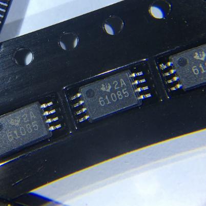
The TXB0108PWR is the TSSOP-20 package variant (PW suffix). Other available packages include USON-20 (DQS), VQFN-20 (RGY), VSSOP-20 (DGS), WQFN-20 (RUK), DSBGA-20 (YZP), and NFBGA-20 (NME). The TSSOP-20 is the most commonly used package for prototyping and production due to its reasonable pin pitch (0.65mm) and ease of assembly.
Key specifications: maximum propagation delay 9.5ns at 1.8V, quiescent current 4uA typical (10uA max over temperature), output drive current +/-20uA DC, +/-15kV ESD protection on B port, 2000V HBM on A port, 1000V CDM on both ports, latch-up exceeds 100mA, operating temperature -40C to 85C.





 English
  简体中文
简体中文  Español
  العربية