TLC2252CDR


双轨至轨输出微功率运算放大器,高级 LinCMOS,4.4-16V,SOIC-8,35µA/ch,卷带包装

300

有效库存
转到查询

Image for reference only

制造商零件:

TLC2252CDR

包装:

SOIC-8(4.9 x 3.9 毫米)

品牌:
您可能感兴趣的其他建议.
说明

The TLC2252CDR is the tape and reel (2500/reel) packaged version of the TLC2252CD dual rail-to-rail output micropower operational amplifier from Texas Instruments in an SOIC-8 package. Electrically identical to the TLC2252CD, the R suffix denotes tape and reel packaging for automated SMT production. Built on Advanced LinCMOS process, it features 35 µA/channel supply current, 200 kHz GBW, 0.12 V/µs slew rate, input bias current of 1 pA typical, and 19 nV/√Hz input noise at 1 kHz. The input common-mode range includes the negative rail and the output swings to both supply rails. Supply range: 4.4V-16V (single) or ±2.2V to ±8V (dual). Commercial temperature range: 0°C to +70°C. Offset voltage: 1.5 mV max (850 µV for A-grade). Ideal for battery-powered instrumentation, high-impedance sensor conditioning, and ADC buffering.

The TLC2252CDR is the tape and reel packaged version of the TLC2252CD dual rail-to-rail output very low-power operational amplifier from Texas Instruments. Built on the Advanced LinCMOS process, it is electrically identical to the TLC2252CD tube-packaged variant, with the R suffix indicating tape and reel packaging (2,500 units per reel) for automated SMT pick-and-place production.

The TLC2252 features rail-to-rail output swing that includes both supply rails, maximizing dynamic range in single-supply or split-supply configurations. The common-mode input voltage range extends to the negative rail (V-), enabling direct ground-referenced sensing in single-supply systems. Each channel consumes only 35 µA of supply current (typical), making it one of the lowest-power dual op-amps available in its class.

Key specifications include a gain-bandwidth product of 200 kHz, a slew rate of 0.12 V/µs, input offset voltage of 1.5 mV max (850 µV for the A-grade TLC2252A), input bias current of 1 pA typical (60 pA max), and equivalent input noise of 19 nV/√Hz at 1 kHz. The low input bias current, a characteristic of the CMOS input stage, makes the TLC2252 ideal for high-impedance signal conditioning from sources such as piezoelectric transducers, photodiodes, and pH probes.

The CDR suffix breaks down as: C = commercial temperature grade (0°C to +70°C), D = SOIC-8 package, R = tape and reel packaging. The tape and reel format is the preferred choice for volume SMT manufacturing, offering 2,500 units per 13-inch reel with consistent orientation for automated pick-and-place equipment. Compared to the tube-packaged TLC2252CD (75 units per tube), the CDR variant reduces per-unit handling cost and eliminates tube-to-reel conversion steps in production.

The TLC2252CDR supports both single-supply (4.4V to 16V) and dual-supply (±2.2V to ±8V) operation, providing flexibility across a wide range of analog signal conditioning applications. It is fully interchangeable with the TLC2252CD in any circuit design, differing only in packaging format.

Compared to earlier generation micropower CMOS op-amps such as the TLC27L2 or TS27L2, the TLC2252 offers significantly improved noise performance (19 nV/√Hz vs typical >50 nV/√Hz), rail-to-rail output for increased dynamic range, and lower input offset voltage. For precision applications requiring tighter offset, the TLC2252ACDR variant offers 850 µV max offset at 25°C in the same tape and reel format.
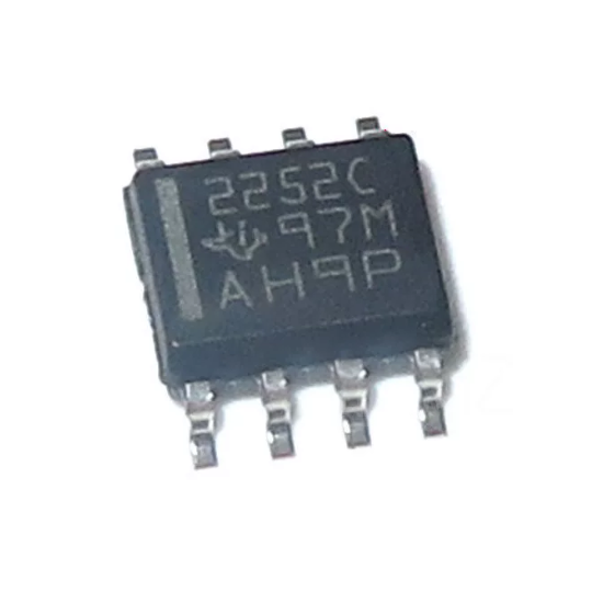

The TLC2252CDR operates as a dual-channel CMOS operational amplifier using Texas Instruments Advanced LinCMOS process, combining micropower consumption with rail-to-rail output capability. It is electrically identical to the TLC2252CD; the R suffix denotes tape and reel packaging only.

CMOS Input Stage: The input stage uses a differential pair of P-channel MOSFETs, providing extremely high input impedance (typically 10^12 Ω) and very low input bias current (1 pA typical). This CMOS input architecture eliminates the input bias current errors that plague bipolar op-amps in high-impedance circuits. The input common-mode voltage range extends from the negative rail (V-) to approximately 1.2V below the positive rail (V+), enabling ground-referenced operation in single-supply applications. The input offset voltage is laser-trimmed to 850 µV max (A-grade) or 1.5 mV max (standard grade) at 25°C.

Rail-to-Rail Output Stage: The output stage uses a complementary CMOS push-pull configuration with both P-channel and N-channel output transistors. This architecture allows the output to swing to within millivolts of both supply rails under light load conditions (typically 10 mV from V- and 60 mV from V+ with 100 kΩ load). The rail-to-rail output maximizes the usable signal range in single-supply applications, which is critical when interfacing with ADCs where even a few hundred millivolts of lost dynamic range can significantly reduce resolution.

Micropower Operation: The TLC2252 achieves its very low supply current (35 µA per channel, 80 µA total for dual) through careful biasing of the internal gain stages at very low quiescent current levels. This micropower design makes the device ideal for battery-powered applications where supply current must be minimized. The trade-off for low power is reduced bandwidth (200 kHz GBW) and slew rate (0.12 V/µs), which are adequate for DC and low-frequency signal conditioning.

Gain-Bandwidth Product: The 200 kHz gain-bandwidth product defines the frequency at which the open-loop gain drops to unity (0 dB). For a closed-loop gain of 10 (20 dB), the bandwidth is approximately 20 kHz; for a gain of 100 (40 dB), approximately 2 kHz. The TLC2252 is therefore best suited for DC and low-frequency applications such as sensor signal conditioning, transducer amplification, and active filtering below audio frequencies.

Slew Rate: The 0.12 V/µs slew rate limits the maximum output swing at high frequencies. For a full-scale sine wave output, the maximum frequency before slew-rate limiting is f_max = SR / (2π × Vp), where Vp is the peak output voltage. For a 5V peak-to-peak output (Vp = 2.5V), the maximum frequency is approximately 7.6 kHz. This is consistent with the device target application space of DC and low-frequency signal conditioning.

Noise Performance: The TLC2252 achieves 19 nV/√Hz input-referred voltage noise at 1 kHz, which is approximately four times lower than competing micropower CMOS op-amps. This improvement is achieved through optimized input transistor sizing and bias current distribution. The low noise, combined with the high input impedance, makes the device excellent for amplifying small signals from high-impedance sources such as piezoelectric sensors and photodiodes without significant noise degradation.

针脚 名称 类型 默认功能 说明
1 1OUT O Channel 1 Output Output of amplifier channel 1; rail-to-rail swing
2 1IN- I Channel 1 Inverting Input Inverting input of amplifier channel 1; high-impedance CMOS input
3 1IN+ I Channel 1 Non-Inverting Input Non-inverting input of amplifier channel 1; common-mode range includes V-
4 V- P Negative Supply / GND Negative power supply (dual supply) or ground (single supply); 0V in single-supply config
5 2IN+ I Channel 2 Non-Inverting Input Non-inverting input of amplifier channel 2
6 2IN- I Channel 2 Inverting Input Inverting input of amplifier channel 2
7 2OUT O Channel 2 Output Output of amplifier channel 2; rail-to-rail swing
8 V+ P 积极供应 Positive power supply; 4.4V to 16V single supply or up to ±8V dual supply
应用 说明
Battery-Powered Instrumentation Micropower op-amp for portable medical devices, handheld meters, and field instruments where 35 µA/ch supply current extends battery life significantly
Sensor Signal Conditioning High-impedance input (1 pA bias current) ideal for piezoelectric transducers, photodiodes, pH electrodes, and other high-Z sensors requiring minimal input loading
ADC Input Buffering Rail-to-rail output maximizes ADC dynamic range in single-supply data acquisition systems; drives ADC sample-and-hold capacitors directly
Portable Monitoring Remote sensing and environmental monitoring nodes where ultra-low quiescent current and wide supply range (4.4-16V) enable long unattended operation
Low-Frequency Active Filtering 200 kHz GBW suitable for active low-pass, band-pass, and notch filters in DC and low-frequency signal paths below audio range
模型 制造商 兼容性 主要区别
TLC2252CD TI 引脚兼容/电气相同 Tube packaging (75/tube) instead of tape and reel; same silicon and specs; preferred for prototyping or low-volume
TLC2252ACDR TI 针脚兼容 A-grade with tighter offset voltage (850 µV max vs 1.5 mV); same tape and reel format; for precision applications
TLV2252CDR TI 针脚兼容 Lower minimum supply voltage (2.7V vs 4.4V); optimized for 3V/5V operation; same rail-to-rail output and low power
TLC27L2CDR TI 针脚兼容 Predecessor device; higher noise, no rail-to-rail output; TLC2252 is recommended upgrade per TI
MCP6022-I/SN 微型芯片 功能相似 Dual rail-to-rail op-amp, 1.8-6V supply, 10 MHz GBW; much wider bandwidth but higher supply current (1 mA/ch)
推荐部件
PMIC for AM335x, 3 bucks, 2 LDOs, battery charger, WLED, I2C, VQFN-48

品牌:

封装:

VQFN-48 (6×6 mm, 0.4 mm pitch)
有库存:
8909pcs

货运周期:3~7 天
最低订购量为 1

转到查询
Octal D-type flip-flop, edge-triggered, async clear, 28MHz, SOP-20

品牌:

封装:

SOP-20 (NS) (12.6×7.8 mm)
有库存:
8359pcs

货运周期:3~7 天
最低订购量为 1

转到查询
3-to-8 decoder/demux, active-low outputs, 3 enable inputs, 15ns, PDIP-16

品牌:

封装:

PDIP-16 (24.33×9.4 mm, Through-Hole)
有库存:
11952pcs

货运周期:3~7 天
最低订购量为 1

转到查询
2W mono Class-AB audio amp, BTL speaker + SE headphone, 2.5-5.5V, HVSSOP-8

品牌:

封装:

HVSSOP-8 (DGN) (3.0×4.9 mm, PowerPAD)
有库存:
3337pcs

货运周期:3~7 天
最低订购量为 1

转到查询
10/100 Ethernet PHY, MII/RMII/SNI, Auto-MDIX, 270mW, LQFP-48, commercial

品牌:

封装:

LQFP-48 (7×7 mm)
有库存:
14754pcs

货运周期:3~7 天
最低订购量为 1

转到查询
Octal bus transceiver, 3-state outputs, 2-6V, 12ns tpd, TSSOP-20

品牌:

封装:

TSSOP-20 (6.5×6.4 mm)
有库存:
2638pcs

货运周期:3~7 天
最低订购量为 1

转到查询
质量保证

我们从合作供应链采购的所有电子元件都经过严格的进货检验。通过仔细的测试,我们确保交付给客户的所有产品都是原装正品,符合质量要求。此外,我们还保存完整的检验记录,使整个供应链流程清晰可查。.

认证
我们获得了多项专业认证,并建立了自己的专业检测实验室,确保交付给客户的每一件产品都符合最高质量要求。我们严格按照流程进行检测,确保产品质量稳定、参数准确。为保证原装正品,我们还与可靠的第三方检测机构合作,进行严格的质量检测。我们始终高度重视质量,完全符合行业标准、相关法规和 ISO 9001:2015 的要求。.

发货与付款

我们从合作供应链采购的所有电子元件都经过严格的进货检验。通过仔细的测试,我们确保交付给客户的所有产品都是原装正品,符合质量要求。此外,我们还保存完整的检验记录,使整个供应链流程清晰可查。.

认证
我们获得了多项专业认证,并建立了自己的专业检测实验室,确保交付给客户的每一件产品都符合最高质量要求。我们严格按照流程进行检测,确保产品质量稳定、参数准确。为保证原装正品,我们还与可靠的第三方检测机构合作,进行严格的质量检测。我们始终高度重视质量,完全符合行业标准、相关法规和 ISO 9001:2015 的要求。.

服务与包装

我们从合作供应链采购的所有电子元件都经过严格的进货检验。通过仔细的测试,我们确保交付给客户的所有产品都是原装正品,符合质量要求。此外,我们还保存完整的检验记录,使整个供应链流程清晰可查。.

认证
我们获得了多项专业认证,并建立了自己的专业检测实验室,确保交付给客户的每一件产品都符合最高质量要求。我们严格按照流程进行检测,确保产品质量稳定、参数准确。为保证原装正品,我们还与可靠的第三方检测机构合作,进行严格的质量检测。我们始终高度重视质量,完全符合行业标准、相关法规和 ISO 9001:2015 的要求。.



