TLC2252AIDR


Dual rail-to-rail CMOS op amp, 35uA/ch, 210kHz GBW, 19nV/rtHz, SOIC-8, -40~125C

6799

有效库存
转到查询

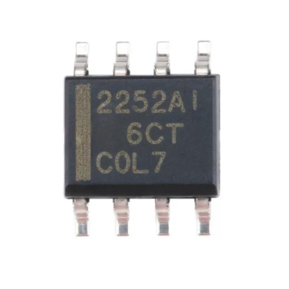
Image for reference only

制造商零件:

TLC2252AIDR

包装:

SOIC-8 (4.9 x 3.9 x 1.5 mm)

品牌:
您可能感兴趣的其他建议.
说明

The TLC2252AIDR is a dual Advanced LinCMOS rail-to-rail output op amp from TI in SOIC-8 (4.9×3.9mm). Ultra-low power: 35uA/ch typical at 5V. Rail-to-rail output with 10mV/60mV headroom from rails. Input common-mode includes negative rail. GBW: 210kHz, slew rate: 0.12V/us. 1pA input bias current, 850uV max Vos (A version), 19nV/rtHz noise at 1kHz. CMRR: 83dB, gain: 124dB. Supply: 4.4V-16V (single) or +/-2.2V to +/-8V (dual). -40C to +125C. MSL-1, RoHS3, EAR99. Tape and Reel, 2500/reel. Upgrade for TLC27L2/L4 and TS27L2/L4.

The TLC2252AIDR is a dual-channel rail-to-rail output CMOS operational amplifier from Texas Instruments, part of the Advanced LinCMOS family. It is specifically designed for very low-power, single-supply or split-supply applications where rail-to-rail output swing and high input impedance are critical. The device is housed in an 8-pin SOIC package.

Each channel consumes only 35 uA of supply current (typical at 5V), making the TLC2252AIDR one of the most power-efficient dual op amps in its class. Despite this ultra-low power consumption, the device delivers a gain bandwidth product of 210 kHz and a slew rate of 0.12 V/us. The input bias current is an exceptionally low 1 pA (typical), making the amplifier ideal for interfacing with high-impedance sources such as piezoelectric transducers, photodiodes, and pH electrodes.

The output stage swings rail-to-rail, meaning the output voltage can approach both the positive and negative supply rails with minimal headroom. The output swing headroom is typically 10 mV from the negative rail and 60 mV from the positive rail at light loads, providing maximum dynamic range in single-supply applications.

The input common-mode voltage range includes the negative rail and extends to within 0.8V of the positive rail, allowing ground-sensing applications in single-supply configurations. The TLC2252A variant (indicated by the A suffix in TLC2252AIDR) provides enhanced precision with a maximum input offset voltage of 850 uV at 25C, compared to 1.5 mV for the standard TLC2252.

Key specifications at 5V single supply: gain bandwidth product 210 kHz (typical), slew rate 0.12 V/us (typical), input voltage noise 19 nV/sqrt(Hz) at 1 kHz, CMRR 83 dB (typical), open-loop voltage gain 124 dB (typical). The device operates from a total supply voltage of 4.4V to 16V (single supply) or +/-2.2V to +/-8V (dual supply). The operating temperature range is -40C to +125C.

The A suffix denotes the enhanced-precision version with lower offset voltage. The I suffix denotes the SOIC-8 package. The D suffix denotes the SOIC package type. The R suffix denotes tape and reel packaging (2,500 units per reel). The TLC2252AIDR is RoHS3 compliant, MSL Level 1 (unlimited), and EAR99 classified.

This device is an excellent performance upgrade for the TS27L2/L4 and TLC27L2/L4 op amps, offering increased output dynamic range, lower noise voltage, and lower input offset voltage in the same package footprint.

The TLC2252AIDR operates as a dual-channel CMOS operational amplifier with rail-to-rail output capability, optimized for ultra-low power consumption and high input impedance.

CMOS Input Stage: The input stage uses PMOS differential pairs, providing the extremely low input bias current of 1 pA (typical). This is several orders of magnitude lower than bipolar input op amps, making the TLC2252AIDR ideal for applications where the source impedance is high (above 100 kohm). The PMOS input pair also allows the common-mode input voltage range to include the negative supply rail, enabling ground-sensing in single-supply circuits. The input common-mode range extends from 0.3V below the negative rail to within approximately 0.8V of the positive rail. The input offset voltage is laser-trimmed to 850 uV maximum (A version) at 25C, with a typical drift of only 0.5 uV/C, ensuring stability over temperature.

Rail-to-Rail Output Stage: The output stage uses a complementary PMOS/NMOS push-pull configuration that allows the output to swing to within millivolts of both supply rails. Unlike many op amps that use a common-emitter output stage requiring at least 1-2V of headroom, the CMOS output stage behaves as a low-resistance switch between the output and the supply rails when the output is near the rails. The output swing headroom is typically 10 mV from the negative rail and 60 mV from the positive rail at light loads (RL = 100 kohm). At heavier loads (RL = 10 kohm), the headroom increases to approximately 30-100 mV. The output can source or sink up to 8 mA (typical) while maintaining good linearity.

Frequency Compensation and Stability: The TLC2252A is internally compensated for unity-gain stability, with a gain-bandwidth product of 210 kHz and a phase margin sufficient for stable operation in voltage-follower (unity gain) configuration. The device can drive capacitive loads up to several hundred picofarads without oscillation. For larger capacitive loads, a small series output resistor (50-100 ohm) isolates the capacitive load from the output stage, maintaining stability.

Power Supply Operation: The device operates over a wide supply voltage range: 4.4V to 16V total (single supply) or +/-2.2V to +/-8V (dual supply). The quiescent supply current per channel is 35 uA (typical at 5V), with a maximum of 80 uA per amplifier across the full temperature range. The total supply current for both channels is therefore typically 70 uA, making the device suitable for battery-powered applications where micropower operation is essential. The device is fully specified at both 5V single supply and +/-5V dual supply.

Noise Performance: The input voltage noise density is 19 nV/sqrt(Hz) at 1 kHz, which is four times lower than competitive micropower CMOS op amps. The input current noise density is typically 0.6 fA/sqrt(Hz), negligible for most applications. The relatively low voltage noise combined with the ultra-low current noise makes the TLC2252AIDR excellent for amplifying signals from high-impedance sources where the noise contribution from the amplifier should not dominate the source noise.

Channel Isolation: The two amplifier channels share the same supply pins but are otherwise independent. The channel-to-channel crosstalk isolation is typically better than 80 dB at low frequencies, ensuring that signals in one channel do not corrupt signals in the other channel.

针脚 名称 类型 说明
1 1OUT 输出 Channel 1 output; rail-to-rail swing; can source/sink up to 8 mA typical
2 1IN- 输入 Channel 1 inverting input; 1 pA typical input bias current; 850 uV max offset voltage (A version)
3 1IN+ 输入 Channel 1 non-inverting input; common-mode range includes negative rail
4 VSS/GND 电源 Negative supply or ground (single supply); connect to system ground or negative rail
5 2IN+ 输入 Channel 2 non-inverting input; common-mode range includes negative rail
6 2IN- 输入 Channel 2 inverting input; 1 pA typical input bias current
7 2OUT 输出 Channel 2 output; rail-to-rail swing; can source/sink up to 8 mA typical
8 VDD 电源 Positive supply; 4.4V to 16V total supply (single) or up to +/-8V (dual); bypass with 0.1 uF ceramic
应用 说明
Piezoelectric Sensor Conditioning 1 pA input bias current prevents loading of high-impedance piezo elements; low 19 nV/rtHz noise preserves small signal integrity; rail-to-rail output maximizes dynamic range in single-supply configurations
Battery-Powered Instrumentation 35 uA per channel supply current enables 24/7 operation on coin-cell or small Li-Ion batteries; 850 uV max offset ensures measurement accuracy in handheld meters and portable sensors
ADC Input Buffer Rail-to-rail output swing maximizes ADC input dynamic range; low offset voltage prevents DC error accumulation; 210 kHz GBW sufficient for buffering low-frequency ADC inputs
pH and Electrochemical Sensors Ultra-low 1 pA input bias current eliminates offset errors from sensor source impedance (often >100 Mohm); ground-sensing input range allows single-supply operation with ground-referenced sensors
Remote Sensing and IoT Micropower operation allows operation from harvested energy or long-life batteries; 0.5 uV/C offset drift maintains accuracy over wide temperature swings in outdoor deployments
模型 制造商 兼容性 主要区别
TLC2252IDR TI Pin-Compatible / Same Package Standard version without A suffix; higher max Vos (1.5 mV vs 850 uV); same GBW, Iq, and noise; lower cost for non-precision applications
TLC2254AIDR TI 功能相似 Quad-channel version; same electrical specifications; 14-pin SOIC package; for multi-channel designs
MCP6002-I/SN 微型芯片 功能相似 Dual CMOS op amp; lower supply range (1.8-6V); 1 MHz GBW; higher Iq (100 uA/ch); different pinout (MSOP-8)
OPA2340PA TI 功能相似 Dual rail-to-rail CMOS op amp; 5.5 MHz GBW; higher Iq (750 uA/ch); DIP-8 package; higher speed applications
TLV2462AIDR TI 功能相似 Dual low-power RRIO op amp; 6.4 MHz GBW; higher Iq (500 uA/ch); for applications needing more bandwidth
推荐部件
3-16S battery monitor/protector, Li-Ion/LiFePO4, 2 ADCs, TQFP-48

品牌:

封装:

TQFP-48 (7 x 7 x 1.0 mm)
有库存:
2150pcs

货运周期:3~7 天
最低订购量为 1

转到查询
I2C 4.5A 1-cell Li-ion charger, NVDC power path, USB OTG, VQFN-24

品牌:

封装:

VQFN-24 (4.0 x 4.0 x 0.75 mm, with thermal pad)
有库存:
4182pcs

货运周期:3~7 天
最低订购量为 1

转到查询
Single micropower RRIO op-amp, 2.7-10V, 65kHz, 11uA, SOT-23-5

品牌:

封装:

SOT-23-5 (2.9 x 2.8 x 1.15 mm)
有库存:
8750pcs

货运周期:3~7 天
最低订购量为 1

转到查询
Single 2-input AND gate, 1.65-5.5V, 24mA drive, SOT-23-5, LVC

品牌:

封装:

SOT-23-5 (2.9 x 1.6 x 1.15 mm)
有库存:
35000 件

货运周期:3~7 天
最低订购量为 1

转到查询
8-bit parallel-load shift register, PISO, 2-6V, 24 MHz, SOIC-16

品牌:

封装:

SOIC-16 (9.9 x 6.0 mm)
有库存:
4837pcs

货运周期:3~7 天
最低订购量为 1

转到查询
Quad differential line receiver, EIA-422/423, 3-state TTL outputs, 5V, SOIC-16

品牌:

封装:

SOIC-16 (9.9 x 6.0 mm)
有库存:
0 件

货运周期:3~7 天
最低订购量为 1

转到查询
质量保证

我们从合作供应链采购的所有电子元件都经过严格的进货检验。通过仔细的测试,我们确保交付给客户的所有产品都是原装正品,符合质量要求。此外,我们还保存完整的检验记录,使整个供应链流程清晰可查。.

认证
我们获得了多项专业认证,并建立了自己的专业检测实验室,确保交付给客户的每一件产品都符合最高质量要求。我们严格按照流程进行检测,确保产品质量稳定、参数准确。为保证原装正品,我们还与可靠的第三方检测机构合作,进行严格的质量检测。我们始终高度重视质量,完全符合行业标准、相关法规和 ISO 9001:2015 的要求。.

发货与付款

我们从合作供应链采购的所有电子元件都经过严格的进货检验。通过仔细的测试,我们确保交付给客户的所有产品都是原装正品,符合质量要求。此外,我们还保存完整的检验记录,使整个供应链流程清晰可查。.

认证
我们获得了多项专业认证,并建立了自己的专业检测实验室,确保交付给客户的每一件产品都符合最高质量要求。我们严格按照流程进行检测,确保产品质量稳定、参数准确。为保证原装正品,我们还与可靠的第三方检测机构合作,进行严格的质量检测。我们始终高度重视质量,完全符合行业标准、相关法规和 ISO 9001:2015 的要求。.

服务与包装

我们从合作供应链采购的所有电子元件都经过严格的进货检验。通过仔细的测试,我们确保交付给客户的所有产品都是原装正品,符合质量要求。此外,我们还保存完整的检验记录,使整个供应链流程清晰可查。.

认证
我们获得了多项专业认证,并建立了自己的专业检测实验室,确保交付给客户的每一件产品都符合最高质量要求。我们严格按照流程进行检测,确保产品质量稳定、参数准确。为保证原装正品,我们还与可靠的第三方检测机构合作,进行严格的质量检测。我们始终高度重视质量,完全符合行业标准、相关法规和 ISO 9001:2015 的要求。.



