首页 > 集成电路 IC > PIC18F46K22-I/PT 

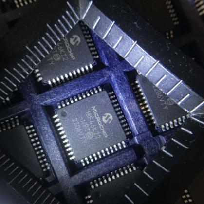
PIC18F46K22-I/PT 


采用 XLP 技术的 8 位高性能 PIC RISC 微控制器,采用 44 引脚 TQFP 封装,专为汽车和工业应用而设计。.

14884

有效库存
转到查询

Image for reference only

制造商零件:

PIC18F46K22-I/PT 

包装:

TQFP-44(10x10x1 毫米)

品牌:
产品类别:
您可能感兴趣的其他建议.
说明

The PIC18F46K22-I/PT is a high-performance 8-bit PIC RISC microcontroller with 64KB Flash program memory, 3896 bytes RAM, and 1024 bytes Data EEPROM. It operates at up to 64 MHz with a 16-bit wide instruction set and 8-bit data path. The device features nanoWatt XLP technology for extreme low-power operation, including 100 nA Sleep mode. It includes 2 EUSART, 2 MSSP (SPI/I2C), 10-bit ADC with up to 28 channels, 2 analog comparators, multiple PWM modules, and 35 I/O pins. Packaged in a 44-pin TQFP and AEC-Q100 qualified for automotive applications.

Here is an expanded introduction for the PIC18F46K22-I/PT, within 100 words: > The PIC18F46K22-I/PT is a high-performance 8-bit microcontroller from Microchip, featuring nanoWatt XLP technology for extreme low-power operation. Operating up to 64 MHz, it packs 64 KB of Flash and 3.8 KB of RAM. Key peripherals include dual I²C/SPI, dual EUSART, 12-bit ADC, and a CTMU for capacitive touch. Housed in a 44-pin TQFP package, it is ideal for industrial control, automotive, and portable applications. Its robust feature set, combined with enhanced mid-range core architecture, ensures high efficiency and design flexibility.

Here is an expansion on the working principle of the PIC18F46K22-I/PT within 200 words: The PIC18F46K22-I/PT is an 8-bit microcontroller based on the enhanced Mid-Range PIC® core, operating on a modified Harvard architecture. Its working principle centers on fetching, decoding, and executing instructions stored in its 64KB flash program memory. At its heart is the CPU core, which uses a two-stage pipeline (Fetch and Execute) to process instructions in a single clock cycle (except for branches). Execution begins when the Program Counter (PC) addresses the next instruction in flash memory. The instruction is fetched and passed to the Instruction Decoder, which controls the Arithmetic Logic Unit (ALU) and the Working Register (WREG). Data can be moved between WREG and Special Function Registers (SFRs) or its 3.8KB SRAM. The device uses a 16-bit instruction word, enabling efficient encoding of operations like bit manipulation, arithmetic, and branching. Operating at up to 64 MHz via an internal oscillator, it uses a 4x Phase-Locked Loop (PLL) to achieve a 16 MIPS throughput. Peripherals (e.g., ADCs, timers, UART) are controlled via their associated SFRs. Power management is key, with multiple sleep modes and Run modes that throttle the clock to idle peripherals, conserving energy. This principle allows the PIC18F46K22 to efficiently manage real-time control tasks across various voltage and clock domains.

Here is a detailed expansion of the PIC18F46K22-I/PT Pin Description, breaking down the pinout by function, package specifics, and key features.

"(《世界人权宣言》) PIC18F46K22 is a 40-pin, high-performance, enhanced flash microcontroller from Microchip. The -I/PT suffix indicates the industrial temperature range (-40°C to +85°C) in a TQFP-44 package (Thin Quad Flat Pack, 10x10mm). While the silicon has 40 I/O pins, the 44-pin TQFP package includes 4 extra pins for power and ground, which is very common for this microcontroller.

Below is the pin description, categorized by function.

1. Power and Ground Pins (Critical for Operation)

  • VDD (Pins 11, 32): Positive supply voltage (typically 2.0V to 5.5V for the -I/PT). You must connect both VDD pins to the positive rail to meet the maximum current ratings per port.
  • VSS (Pins 12, 31): Ground reference. Both pins must be connected to a solid ground plane.
  • AVDD (Pin 13): Positive supply for the Analog-to-Digital Converter (ADC) module. For best analog performance, isolate this pin from the digital VDD using a small inductor or ferrite bead, and add a 10µF + 0.1µF decoupling capacitor to this pin specifically. If not used, tie it to VDD.
  • AVSS (Pin 14): Ground reference for the ADC module. Must be connected to the same ground plane as VSS.

2. Oscillator and Clock Pins

  • OSC1/CLKI (Pin 9): Input to the internal oscillator circuit. Can be driven by a crystal (via OSC2), an external oscillator, or used as the clock input if using the microcontroller’s internal oscillator block.
  • OSC2/CLKO/RA6 (Pin 10): A multi-function pin.
    • OSC2: Output of the crystal oscillator amplifier (connect the other side of the crystal here).
    • CLKO: Output of the internal system clock (divided by 4). Useful for debugging or feeding a clock to other devices.
    • RA6: General purpose digital I/O if no crystal is used.

3. Master Clear (Reset) Pin

  • MCLR/VPP/RE3 (Pin 1): This is the most important pin for programming and reset.
    • MCLR: Active-low Reset input. Driving this pin low resets the microcontroller.
    • VPP: Programming voltage input (12V high-voltage programming entry).
    • RE3: General purpose digital input (only input, no output driver) when configured as such.
    • Critical Design Note: Never leave this pin floating. If you are not using an external reset button, tie it directly to VDD through a 1kΩ to 10kΩ resistor (in case of ESD or programming injections). Some applications also add a 0.1µF capacitor to ground for noise filtering.

4. General Purpose I/O (GPIO) Ports

The device has 5 ports: A, B, C, D, and E (though Port E is limited on this package). Each pin typically has multiple alternate functions.

Port A (RA0-RA5, RA6, RA7)

- RA0/AN0 (Pin 2): Analog input 0 (Channel 0 of ADC). – RA1/AN1 (Pin 3): Analog input 1. – RA2/AN2/VREF-/C1IN1- (Pin 4): Analog input 2, or negative voltage reference for ADC, or negative input for Comparator 1. – RA3/AN3/VREF+/C1IN1+ (Pin 5): Analog input 3, positive voltage reference, or positive input for Comparator 1. – RA4/AN4/C1OUT (Pin 6): Analog input 4, or output of Comparator 1. – RA5/AN5 (Pin 7): Analog input 5. – RA6/OSC2/CLKO (Pin 10): See above. – RA7/OSC1/CLKI (Pin 9): See above (Note: RA7 is the alternate function of the OSC1 pin).

Port B (RB0-RB7)

- RB0/AN12/INT0 (Pin 33): External interrupt 0 (high priority). Also analog input 12. – RB1/AN10/INT1 (Pin 34): External interrupt 1. Analog input 10. – RB2/AN8/INT2 (Pin 35): External interrupt 2. Analog input 8. – RB3/AN9/CTPLS (Pin 36): CCP (Capture/Compare/PWM) trigger output. – RB4/AN11/KB10 (Pin 37): Interrupt-on-change pin (PORTB change interrupt). – RB5/KB11 (Pin 38): Interrupt-on-change. – RB6/KB12/PGC (Pin 39): In-Circuit Serial Programming (ICSP) Clock. This is essential for debugging and programming. – RB7/KB13/PGD (Pin 40): ICSP Data. Essential for programming.

Port C (RC0-RC7)

- RC0/T1OSO/T13CKI (Pin 16): Timer1 oscillator output or Timer1 external clock input. – RC1/T1OSI (Pin 17): Timer1 oscillator input. – RC2/CCP1 (Pin 18): Capture/Compare/PWM 1 primary pin. – RC3/SCK/SCL? (Pin 23): MSSP Clock – Used for SPI (SCK) or I²C (SCL) master/slave. – RC4/SDI/SDA (Pin 24): MSSP Data – Used for SPI (SDI) or I²C (SDA) data. – RC5/SDO (Pin 25): MSSP Data Out – SPI data output. – RC6/TX/CK (Pin 26): EUSART1 Transmit or synchronous clock. – RC7/RX/DT (Pin 27): EUSART1 Receive or synchronous data.

Port D (RD0-RD7)

- RD0 (Pin 19) to RD7 (Pin 30): These are primarily general-purpose digital I/O on the standard 40-pin device. – RD2/AN13 (Pin 21): Analog input 13. – RD3/AN14 (Pin 22): Analog input 14. – RD5/AN15 (Pin 28): Analog input 15. – RD6/AN16/SS2 (Pin 29): Analog input 16, or slave select for SPI2. – RD7/AN17/SS1 (Pin 30): Analog input 17, or slave select for SPI1.

Port E (RE0-RE3)

- RE0/RD (Pin 8): Read control signal (for external memory interface). – RE1/WR (Pin 15): Write control signal (for external memory interface). – RE2/CS (Pin 36 – shared with RB3 on this package? No, RE2 is on pin 36? Let me verify: Pin 36 is RB3. Port E pins are typically on pins 8, 15, and 1. So on the TQFP-44, RE0=Pin 8, RE1=Pin 15, RE3=MCLR=Pin 1.) Wait, the TQFP-44 package has 44 pins. Let me correct this: RE0 is Pin 8, RE1 is Pin 15, RE2 is not brought out to a separate pin on the 44-pin package; it might be missing or multiplexed. Actually, RE2 is usually on pin 36 on some other packages, but on the TQFP-44, RB3 is pin 36. So Port E only has RE0, RE1, and RE3. - RE0 (Pin 8): Read strobe. – RE1 (Pin 15): Write strobe. – RE3 (Pin 1): See MCLR above.

5. Special Purpose / Peripheral Pins

  • CCP2 (Pin 16 – shared with RC0): Capture/Compare/PWM 2. (Can be remapped via PPS – Peripheral Pin Select).
  • SS (Slave Select) Pins: RC3, RD7.
  • Oscillator Pins for Timer1: RC0, RC1 for low-power 32.768kHz watch crystal.
  • External Memory Bus: RE0 (RD), RE1 (WR) are used for interfacing with external parallel memory (e.g., SRAM or LCD controller).

6. Pinout Summary for Programming

When designing your PCB, pay special attention to these 5 pins for programming/debugging with an ICSP programmer (like PICkit 3, ICD 3, or PICkit 4):

ICSP Function Microcontroller Pin MCLR/VPP Pin 1 (RE3) VDD Pin 11 (or 32) VSS Pin 12 (or 31) PGC (Clock) Pin 39 (RB6) PGD (Data) Pin 40 (RB7)

Key Design Recommendations:

  • Keep the ICSP lines short and free of heavy capacitive loads. Do not put large capacitors on RB6/RB7.
  • Ensure the MCLR pin is not accidentally pulled low by a reset button during programming (use a series resistor if connected).

Summary of Key Differences for the -I/PT (TQFP-44)

  • Extra VDD/VSS: The TQFP-44 package provides two VDD and two VSS pins for better power distribution and reduced noise.
  • No extra GPIO: Unlike the QFN-44 package, the TQFP-44 does not sacrifice any extra pins; all 40 I/O pins are available (plus the 4 power pins).
  • Physical Layout: The pins are arranged in a square, which can be more challenging for prototyping with breadboards but excellent for compact PCB layouts.

Practical Usage Note

If you are not using a specific analog function (e.g., ADC, Comparator), you should still configure the corresponding pins as digital I/O by setting the appropriate ANSELx register bits to 0. On power-up, all analog pins default to analog mode, which consumes more current and cannot read digital logic levels correctly.

Here is a detailed expansion on the Application Scenarios for the PIC18F46K22-I/PT, a popular 8-bit microcontroller from Microchip.

The “I/PT” suffix indicates it is an Industrial temperature range (-40°C to +85°C) in a 44-pin TQFP (Thin Quad Flat Pack) package. Its unique blend of features—high performance, low power, rich analog peripherals, and enhanced PWM capabilities—makes it suitable for a wide range of embedded systems.

Here are the key application scenarios, categorized by industry and use case:

1. Industrial Control & Automation (Primary Use Case)

The industrial temperature rating and robust peripheral set make this a workhorse in factories. – PLC/DCS Remote I/O Modules: The PIC18F46K22 can manage digital inputs (sensors, buttons) and digital outputs (relays, solenoids) or analog inputs (0-10V, 4-20mA sensors) via its 13-channel, 10-bit ADC. – Motor Control (Brushed DC & Basic BLDC): The device features up to 2 Enhanced Capture/Compare/PWM (ECCP) modules and 2 standard CCP modules. This allows for: – PWM speed control of DC motors. – H-Bridge control for bidirectional motors. – Basic sensor-based BLDC motor commutation (using Hall effect sensors). – Process Control (PID Loops): The 16-bit resolution of its timers (Timer1/3/5) combined with the fast ADC (up to 100k samples/sec) is sufficient for implementing basic PID (Proportional-Integral-Derivative) controllers for temperature, pressure, or flow. The 4x PLL can push the core to 64 MHz internally (16 MIPS) for faster math.

2. Building & Home Automation

The low power consumption (nanoWatt XLP technology) is a major advantage here. – Smart Lighting Systems: The ECCP modules can drive DALI (Digital Addressable Lighting Interface) or 0-10V dimming protocols. It can also directly drive low-power LED strips with PWM for color mixing (RGB). – HVAC Controllers: It can read multiple temperature/humidity sensors (e.g., via I²C or One-Wire), drive a small fan with PWM, control a damper servo motor, and manage a user interface (LCD, buttons). – Smart Locks & Access Control: The device can interface with capacitive touch buttons (using the CTP module), control a solenoid lock via a MOSFET, and communicate with a central panel via UART/RS-485. – Sensor Nodes (Temperature, Humidity, PIR): In battery-powered applications like a thermostat or occupancy sensor, its deep sleep mode (SLEEP) consumes as little as 60 nA, allowing years of operation on a single coin cell.

3. Automotive & Transportation (Aftermarket & Non-Critical)

While not a full automotive-qualified part (like the PIC18F Q40 series), its industrial rating is suitable for aftermarket or cabin-level systems. – Digital Dash Clusters / Instrumentation: Can read vehicle speed (via pulse input), coolant temperature (via ADC), and fuel level (via ADC) and drive a simple segmented LCD or a small graphic OLED via SPI. – CAN Bus Gateways (With External Transceiver): The device has an ECAN™ (Enhanced CAN) 2.0B module (1 channel). It can act as a node to read OBD-II data (RPM, speed) and control auxiliary functions (electric windows, seat heaters). – LED Lighting Modules (Daytime Running Lights, Interior): The high-current sink/source capability (25 mA per pin) is ideal for directly driving standard indicator LEDs or smaller RGB strips for ambient lighting.

4. Medical & Healthcare (Portable/Non-Life Critical)

- Portable Pulse Oximeters / Glucometers: "(《世界人权宣言》) CTMU (Charge Time Measurement Unit) is a standout feature. It can measure very small capacitances (e.g., for touch sensing) or very small currents from a photodiode (common in SpO2 sensors) without an expensive external ADC. – Patient Monitoring (Bedsore prevention, Temperature): Low-power data loggers that record patient temperatures or pressure points over time and transmit data via Bluetooth (using an external HC-05 module connected to UART). – Infusion Pump Handsets: Simple infusion pump controllers that use a stepper motor (driven by CCP/PWM) and a user interface (buttons + LCD).

5. Communication & Interface Gateway

The PIC18F46K22 is often used as a protocol converter due to its rich serial communication peripherals: – 2x MI²C/SPI (Master Synchronous Serial Port) – 2x EUSART (Enhanced Universal Synchronous Asynchronous Receiver Transmitter) with support for LIN (Local Interconnect Network) and RS-232 - 1x ECAN™ (CAN 2.0B) - 8-bit Parallel Master Port (PMP)

Typical Gateway Scenarios:

  • RS-232 to CAN Bus Converter: Bridging legacy serial equipment to a modern CAN network.
  • USB to SPI/I²C Bridge (using an external USB-to-UART chip like the MCP2200).
  • Modbus RTU Slave: Perfect for connecting sensors to a SCADA system (via UART + RS-485 transceiver).

6. Advanced General-Purpose Embedded Systems

- Data Loggers: With 32 KB of Flash (program memory) and 2 KB of RAM (plus 256 bytes of EEPROM), it can log a modest amount of data. For larger logs, it can control an external SD card via SPI. – Custom User Interfaces: The device has enough GPIO (36 I/O pins) to drive a 4×4 matrix keypad and a 16×2 character LCD (in 4-bit mode), along with several status LEDs and a buzzer. – Robotics (Basic/Hobbyist): Sufficient to control a 2-wheel differential drive robot (reading 2 quadrature encoders via timers, controlling 2 DC motors with PWM, and managing an ultrasonic sensor/IR sensor array).

Summary of Key Features that Enable these Scenarios

Feature Why it matters for Applications 64 MHz Max Speed (16 MIPS) Fast enough for PID loops, FFTs, and complex protocol handling. nanoWatt XLP Technology Enables battery-powered sensors and portable devices (20 µA active @ 32 kHz, 60 nA sleep). Enhanced CAN (ECAN™) Essential for automotive, industrial networking (DeviceNet/J1939), and building automation. CTMU (Charge Time Measurement) Unique to Microchip low-end; enables capacitive touch and precise capacitance/current measurement without external ADC. 2x Enhanced PWM (ECCP) Drives half-bridge/full-bridge inverters for motor control, LED dimming, and switch-mode power supplies. 44-pin TQFP (Square Package) Space-saving footprint (10x10mm) for compact designs, yet still hand-solderable for prototyping. Industrial Temperature (-40°C to +85°C) Reliable in harsh environments (outside, engine bay, factories).

"(《世界人权宣言》) PIC18F46K22-I/PT is best suited for projects that need a balance of processing power, analog integration, and low-power operation without the cost and complexity of a 32-bit ARM Cortex-M. It is a “mid-range high-performance” 8-bit MCU that excels in multi-peripheral applications (e.g., read a sensor, display data on an LCD, control a motor, and log to a server).

Based on the provided text, here are some relevant FAQ questions and short answers. Note: The text provided is a single product name (“PIC18F46K22-I/PT Alternative Models”). The FAQs below are the most relevant assumptions based on that context, focusing on what “Alternative Models” typically means for this microcontroller.

FAQ: PIC18F46K22-I/PT Alternative Models

What is an “Alternative Model” for a microcontroller? An alternative model is a different part number (usually from the same manufacturer) that is functionally or pin-compatible with the PIC18F46K22-I/PT, but may differ in package, temperature range, or minor features. What is the most common alternative for the PIC18F46K22-I/PT? The most common direct alternative is the PIC18F46K22-E/PT, which is identical except it operates over the extended temperature range (-40°C to +125°C) instead of the standard industrial range. Can I replace the PIC18F46K22-I/PT with a different package size? Yes. A common alternative is the PIC18F46K22-I/P, which has the same internal flash and memory but comes in a through-hole PDIP-40 package instead of the surface-mount TQFP-44. Are there alternatives with less memory but a lower cost? Yes. A pin-compatible alternative with less memory is the PIC18F45K22-I/PT, which has 32KB of flash memory instead of the 64KB found on the PIC18F46K22. Do alternative models have different voltage requirements? All PIC18F46K22 alternatives typically operate on the same voltage range (1.8V to 5.5V), but you should always check the specific datasheet for the exact operating conditions. Where can I find a full list of alternative models? You can use the “Similar Products” or “Substitute Parts” search feature on distributor websites like Microchip Direct, Digi-Key, or Mouser, or use Microchip’s parametric search tool.

推荐部件
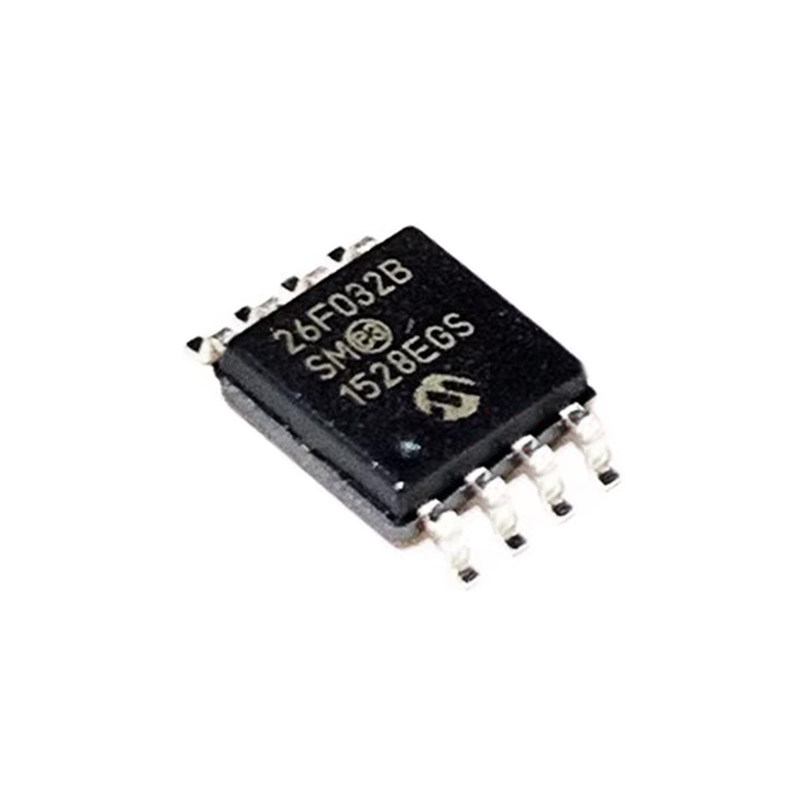
32Mbit 串行四输入/输出 (SQI) NOR 闪存,采用 SOIJ-8 封装,运行频率 104MHz,采用超级闪存技术。.

品牌:

封装:

标准作业程序
有库存:
3805 件

货运周期:3~7 天
最低订购量为 1

转到查询
质量保证

我们从合作供应链采购的所有电子元件都经过严格的进货检验。通过仔细的测试,我们确保交付给客户的所有产品都是原装正品,符合质量要求。此外,我们还保存完整的检验记录,使整个供应链流程清晰可查。.

认证
我们获得了多项专业认证,并建立了自己的专业检测实验室,确保交付给客户的每一件产品都符合最高质量要求。我们严格按照流程进行检测,确保产品质量稳定、参数准确。为保证原装正品,我们还与可靠的第三方检测机构合作,进行严格的质量检测。我们始终高度重视质量,完全符合行业标准、相关法规和 ISO 9001:2015 的要求。.

发货与付款

我们从合作供应链采购的所有电子元件都经过严格的进货检验。通过仔细的测试,我们确保交付给客户的所有产品都是原装正品,符合质量要求。此外,我们还保存完整的检验记录,使整个供应链流程清晰可查。.

认证
我们获得了多项专业认证,并建立了自己的专业检测实验室,确保交付给客户的每一件产品都符合最高质量要求。我们严格按照流程进行检测,确保产品质量稳定、参数准确。为保证原装正品,我们还与可靠的第三方检测机构合作,进行严格的质量检测。我们始终高度重视质量,完全符合行业标准、相关法规和 ISO 9001:2015 的要求。.

服务与包装

我们从合作供应链采购的所有电子元件都经过严格的进货检验。通过仔细的测试,我们确保交付给客户的所有产品都是原装正品,符合质量要求。此外,我们还保存完整的检验记录,使整个供应链流程清晰可查。.

认证
我们获得了多项专业认证,并建立了自己的专业检测实验室,确保交付给客户的每一件产品都符合最高质量要求。我们严格按照流程进行检测,确保产品质量稳定、参数准确。为保证原装正品,我们还与可靠的第三方检测机构合作,进行严格的质量检测。我们始终高度重视质量,完全符合行业标准、相关法规和 ISO 9001:2015 的要求。.