首页 > 集成电路 IC > PIC16F72-I/SP

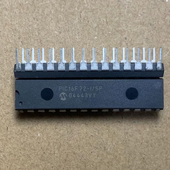
PIC16F72-I/SP


8 位 PIC MCU、2Kx14 闪存、128B RAM、22 个 I/O、5 通道 8 位 ADC、3 个定时器、CCP PWM、SPI/I2C、SPDIP-28、2-5.5V、-40~85C

15000

有效库存
转到查询

Image for reference only

制造商零件:

PIC16F72-I/SP

包装:

SPDIP-28(300 密耳)(35.56 x 7.62 毫米,2.54 毫米间距)

品牌:
产品类别:
您可能感兴趣的其他建议.
说明

The PIC16F72-I/SP from Microchip Technology is an 8-bit CMOS Flash microcontroller based on the PIC mid-range RISC architecture in a 28-pin SPDIP package. Key specifications: 35 single-word instructions; 200 ns instruction cycle at 20 MHz (DC-20 MHz clock input); 2K x 14-bit Flash program memory (3.5 KB); 128 bytes RAM; 22 I/O pins with 25 mA sink/source per pin; 5-channel 8-bit ADC; 3 timers (Timer0: 8-bit with 8-bit prescaler, Timer1: 16-bit with prescaler, Timer2: 8-bit with period register and postscaler); 1 CCP (Capture/Compare/PWM) module with 10-bit PWM resolution; synchronous serial port (MSSP) configurable as SPI master or I2C slave; 8-level hardware stack; watchdog timer with independent on-chip RC oscillator; power-on reset (POR), power-up timer (PWRT), oscillator start-up timer (OST); in-circuit serial programming (ICSP) via 2 pins; power-saving SLEEP mode; operating voltage 2.0 V to 5.5 V; operating temperature -40 to +85 degrees C (I suffix industrial grade); Flash endurance 1000 erase/write cycles typical. The SP suffix denotes 28-pin SPDIP (skinny PDIP, 300 mil) through-hole package with tube packaging. Active product, currently in production at Microchip.

The PIC16F72-I/SP from Microchip Technology is a member of the PIC16F mid-range 8-bit microcontroller family, offering a balanced combination of program memory, peripherals, and I/O in a 28-pin through-hole package. It is particularly well-suited for motor control, power conversion, and industrial control applications due to its CCP module and multiple timers.

The PIC16F72 occupies a sweet spot in the PIC16F product line: more capable than the smaller PIC16F628A (18-pin, no ADC) but less expensive than the larger PIC16F877A (40-pin, 8K Flash). The 2K x 14-bit Flash program memory is sufficient for moderate-complexity control algorithms, and the 128 bytes of RAM supports typical variable storage and stack usage.

The 5-channel 8-bit ADC is a key differentiator over ADC-less PIC devices. With 8-bit resolution and a conversion time of approximately 20 us, it is suitable for monitoring analog sensors such as temperature sensors, potentiometers, and voltage dividers. The 8-bit resolution provides 256 discrete levels over the 0-5 V input range (approximately 20 mV per step), which is adequate for many control and monitoring applications.

The CCP (Capture/Compare/PWM) module is the most important peripheral for motor control and power conversion. In PWM mode, it can generate a 10-bit resolution PWM signal with a period set by Timer2 and a duty cycle set by the CCPR1L register. The 10-bit resolution provides 1024 discrete duty cycle steps, enabling smooth motor speed control and precise power converter output regulation.

The synchronous serial port (MSSP) can be configured as either a 3-wire SPI master or a 2-wire I2C slave. In SPI mode, it can communicate with external ADCs, DACs, EEPROMs, and display drivers. In I2C mode, it can act as a slave device on an I2C bus, responding to commands from a master MCU or host processor.

The PIC16F72 is widely used in the Indian and Chinese electronics markets for motor control applications, particularly in inverter drives for single-phase and three-phase induction motors. Microchip application note AN901 describes a bidirectional V/f control implementation using the PIC16F72.

The I suffix denotes industrial temperature range (-40 to +85 degrees C). The SP suffix denotes the 28-pin SPDIP (skinny PDIP, 300 mil body width) through-hole package. This package is popular for prototyping, educational use, and low-volume production where hand soldering or socket mounting is preferred. The PIC16F72 is also available in SOIC-28 (SO), SSOP-28 (SS), and QFN-28 (ML) packages for surface-mount production.

The 1000 erase/write cycle Flash endurance is relatively low by modern standards (current PIC devices offer 10K-100K cycles). This limits the use of self-programming and field firmware updates. For applications requiring frequent firmware updates, consider newer PIC devices with higher Flash endurance.

The PIC16F72-I/SP operates as an 8-bit Harvard-architecture RISC microcontroller with separate program and data memory buses.

Harvard Architecture: The PIC16F72 uses a modified Harvard architecture where program memory and data memory have separate address spaces and buses. The program memory bus is 14 bits wide (to accommodate 14-bit instructions), while the data memory bus is 8 bits wide. This separation allows simultaneous access to instruction and data, improving throughput compared to von Neumann architectures where instruction and data share the same bus.

RISC Instruction Set: The instruction set consists of only 35 single-word instructions (except for program branches which are two-cycle). Most instructions execute in a single cycle (200 ns at 20 MHz). The instructions are 14 bits wide and include arithmetic (ADD, SUB), logical (AND, OR, XOR), data movement (MOV, SWAP), bit manipulation (BSF, BCF, BTFSS, BTFSC), and control (GOTO, CALL, RETURN, RETLW) operations. The simple instruction set reduces code size and execution time for control-oriented applications.

Pipeline Operation: The PIC16F72 uses a 2-stage pipeline: while one instruction is being executed, the next instruction is being fetched from program memory. This overlapping enables most instructions to execute in a single cycle. Branch instructions (GOTO, CALL) take two cycles because the pipeline must be flushed and refilled with the target instruction.

Program Memory: The 2K x 14-bit Flash program memory stores the application code. The program counter is 13 bits wide, allowing addressing of up to 8K locations (the PIC16F72 uses only 2K of this space). The reset vector is at address 0x0000, and the interrupt vector is at address 0x0004. The Flash is in-circuit serial programmable (ICSP) via the PGD and PGC pins, allowing firmware updates without removing the device from the board.

Data Memory (RAM): The 128 bytes of data memory are organized as a banked register file. The data memory is divided into four banks (Bank 0-3), each up to 128 bytes. Special Function Registers (SFRs) that control the peripherals occupy the lower addresses in each bank. General-Purpose Registers (GPRs) for user variables occupy the upper addresses. The bank is selected by the RP1:RP0 bits in the STATUS register. Most applications use only Bank 0 and Bank 1 for the majority of operations.

8-Level Hardware Stack: The hardware stack stores return addresses for CALL instructions and interrupt service routines. The stack is 13 bits wide (matching the program counter) and 8 levels deep. There is no stack overflow or underflow detection; exceeding 8 nested calls causes the oldest return address to be lost. The stack is not accessible as data memory (unlike some other MCU architectures).

Interrupt System: The PIC16F72 has a single interrupt vector at 0x0004. All interrupt sources share this vector, and the interrupt service routine must poll the interrupt flag bits to determine which source triggered the interrupt. Interrupt sources include: TMR0 overflow, TMR1 overflow, CCP capture/compare, MSSP (SPI/I2C) events, A/D conversion complete, and external INT pin (RB0). The INTCON, PIE1, and PIR1 registers control interrupt enables and flags.

Timer0: 8-bit timer/counter with an 8-bit programmable prescaler (1:2 to 1:256). Can be clocked from the internal instruction cycle clock (FOSC/4) or from an external pin (RA4/T0CKI). The prescaler is shared with the watchdog timer; it can be assigned to either Timer0 or the WDT, but not both simultaneously.

Timer1: 16-bit timer/counter with a programmable prescaler (1:1, 1:2, 1:4, 1:8). Can be clocked from FOSC/4, from an external pin (RC0/T1CKI), or from an external 32.768 kHz crystal oscillator connected to the T1OSO and T1OSI pins. The crystal oscillator option allows Timer1 to serve as a real-time clock that continues running during SLEEP mode.

Timer2: 8-bit timer with an 8-bit period register (PR2) and both a prescaler (1:1, 1:4, 1:16) and postscaler (1:1 to 1:16). Timer2 is primarily used as the PWM time base for the CCP module. When TMR2 equals PR2, it resets on the next cycle and triggers the postscaler.

CCP Module: The Capture/Compare/PWM module operates in three modes. (1) Capture mode: captures the Timer1 value when an event occurs on the RC2/CCP1 pin (rising edge, falling edge, or every 4th/16th rising edge). (2) Compare mode: generates an interrupt or output event when Timer1 matches the CCPR1 register value. (3) PWM mode: generates a PWM signal with 10-bit duty cycle resolution on the RC2/CCP1 pin. The PWM period is set by PR2 and the Timer2 prescaler; the duty cycle is set by the CCPR1L register and the CCP1X:CCP1Y bits.

ADC Module: The 5-channel 8-bit ADC converts an analog input voltage on one of the AN0-AN4 pins (RA0-RA4) to a digital value. The conversion uses a successive approximation algorithm with a conversion time of approximately 20 us at the maximum recommended clock rate. The ADC reference voltage is the supply voltage (VDD). The result is stored in the ADRES register.

MSSP Module: The Master Synchronous Serial Port can be configured as SPI master or I2C slave. In SPI mode, it generates the clock (SCK) and controls data transfer to external SPI devices. In I2C mode, it responds to the I2C slave address, receiving and transmitting data under master control. The I2C implementation supports 7-bit addressing and standard mode (100 kHz).

针脚 名称 类型 说明
1 RA2/AN2/VREF- 输入/输出 Port A bit 2; analog input 2 for ADC; negative voltage reference input (not implemented on PIC16F72); can be used as digital I/O or ADC channel 2; 25 mA sink/source; TTL input levels
2 RA3/AN3/VREF+ 输入/输出 Port A bit 3; analog input 3 for ADC; positive voltage reference input (not implemented on PIC16F72); can be used as digital I/O or ADC channel 3; 25 mA sink/source
3 RA4/T0CKI 输入/输出 Port A bit 4; Timer0 external clock input; open-drain output (requires external pull-up for output operation); ADC channel 4; Schmitt trigger input; the only Port A pin with open-drain output; commonly used as external clock input for Timer0
4 RA5/AN4/SS 输入/输出 Port A bit 5; analog input 4 for ADC; SPI slave select input (SS) when MSSP is configured in SPI slave mode; TTL input levels; 25 mA sink/source; can be used as chip select for SPI communication
5 VSS 地面 Ground connection; connect to PCB ground plane; all digital and analog circuits reference this pin; bypass VDD to VSS with 100 nF ceramic capacitor
6 OSC1/CLKIN 输入 Oscillator crystal input or external clock input; for crystal operation, connect a crystal (up to 20 MHz) between OSC1 and OSC2 with load capacitors; for external clock, apply a 0-5 V clock signal to OSC1 (leaving OSC2 unconnected); the oscillator mode is selected by the FOSC1:FOSC0 configuration bits
7 OSC2/CLKOUT 输出 Oscillator crystal output; connects to the other terminal of the crystal; in RC oscillator mode, outputs the instruction cycle clock (FOSC/4); in external clock mode, leave unconnected
8 VDD 电源 Positive supply voltage; 2.0 V to 5.5 V; all I/O levels are referenced to VDD; bypass with 100 nF ceramic capacitor to VSS close to the pin; supply current is approximately 2 mA at 5 V, 20 MHz (depends on operating mode)
9 RB0/INT 输入/输出 Port B bit 0; external interrupt input; interrupt on rising or falling edge (selected by INTEDG bit); TTL input levels with Schmitt trigger on interrupt path; 25 mA sink/source; interrupt-on-change feature; weak internal pull-up when port is configured as input (controlled by OPTION_REG bit 7)
10 RB1 输入/输出 Port B bit 1; general-purpose I/O; interrupt-on-change feature; internal weak pull-up; 25 mA sink/source; TTL input levels
11 RB2 输入/输出 Port B bit 2; general-purpose I/O; interrupt-on-change feature; internal weak pull-up; 25 mA sink/source; TTL input levels
12 RB3/PGM 输入/输出 Port B bit 3; low-voltage ICSP programming enable (PGM) pin; interrupt-on-change feature; internal weak pull-up; 25 mA sink/source; if LVP configuration bit is enabled, this pin must be held low during normal operation to prevent accidental entry into programming mode
13 RB4 输入/输出 Port B bit 4; interrupt-on-change feature; internal weak pull-up; 25 mA sink/source; TTL input levels; commonly used as interrupt input for external events
14 RB5 输入/输出 Port B bit 5; interrupt-on-change feature; internal weak pull-up; 25 mA sink/source
15 RB6/PGC 输入/输出 Port B bit 6; ICSP programming clock pin; interrupt-on-change feature; internal weak pull-up; 25 mA sink/source; Schmitt trigger input for ICSP; used by MPLAB ICD and PICKit programmers
16 RB7/PGD 输入/输出 Port B bit 7; ICSP programming data pin; interrupt-on-change feature; internal weak pull-up; 25 mA sink/source; Schmitt trigger input for ICSP; used by MPLAB ICD and PICKit programmers
17 RC0/T1OSO/T1CKI 输入/输出 Port C bit 0; Timer1 oscillator output; Timer1 external clock input; 25 mA sink/source; Schmitt trigger input; connect 32.768 kHz crystal between RC0 and RC1 for Timer1 RTC operation
18 RC1/T1OSI 输入/输出 Port C bit 1; Timer1 oscillator input; 25 mA sink/source; Schmitt trigger input; complementary connection for 32.768 kHz crystal
19 RC2/CCP1 输入/输出 Port C bit 2; CCP1 (Capture/Compare/PWM) module I/O; in PWM mode, outputs the PWM waveform; in Capture mode, receives the external trigger signal; in Compare mode, outputs the compare match signal; 25 mA sink/source; Schmitt trigger input
20 RC3/SCK/SCL 输入/输出 Port C bit 3; SPI clock (SCK) in SPI mode; I2C clock (SCL) in I2C slave mode; 25 mA sink/source; Schmitt trigger input; used by the MSSP module for synchronous serial communication
21 RC4/SDI/SDA 输入/输出 Port C bit 4; SPI data input (SDI) in SPI mode; I2C data (SDA) in I2C slave mode; 25 mA sink/source; Schmitt trigger input; receives serial data from external devices
22 RC5/SDO 输入/输出 Port C bit 5; SPI data output (SDO) in SPI mode; 25 mA sink/source; transmits serial data to external devices; not used in I2C mode
23 RC6 输入/输出 Port C bit 6; general-purpose I/O; 25 mA sink/source; Schmitt trigger input; no alternate function on PIC16F72 (USART not available on this device)
24 RC7 输入/输出 Port C bit 7; general-purpose I/O; 25 mA sink/source; Schmitt trigger input; no alternate function on PIC16F72
25 RA0/AN0 输入/输出 Port A bit 0; analog input 0 for ADC; can be used as digital I/O or ADC channel 0; 25 mA sink/source; TTL input levels; the ADC channel assignment is controlled by the CHS2:CHS0 bits in the ADCON0 register
26 RA1/AN1 输入/输出 Port A bit 1; analog input 1 for ADC; can be used as digital I/O or ADC channel 1; 25 mA sink/source; TTL input levels
27 RA6/OSC2 输入/输出 Not available on PIC16F72 in SPDIP-28 package; this pin is bonded to OSC2 internally; not a separate GPIO pin on this package variant
28 RA7/OSC1 输入/输出 Not available on PIC16F72 in SPDIP-28 package; this pin is bonded to OSC1 internally; not a separate GPIO pin on this package variant
应用 说明
Motor Inverter Control (V/f Drive) Single-phase or three-phase induction motor V/f control; CCP module generates 3 PWM channels (with external dead-time logic) for inverter bridge; Timer1 provides timing reference; ADC reads motor current and DC bus voltage; Microchip AN901 describes complete implementation; 2K Flash sufficient for V/f algorithm; popular in low-cost motor drives in Asian markets
Switch-Mode Power Supply (SMPS) PWM generation for buck, boost, or flyback converters; CCP module generates PWM with 10-bit duty cycle resolution; ADC monitors output voltage and current for feedback; Timer2 sets PWM frequency; I2C interface receives setpoint commands from host; 2K Flash sufficient for PID control loop
Industrial Sensor Interface Read multiple analog sensors (temperature, pressure, flow) via 5-channel ADC; process and format data; transmit to host via I2C or SPI; Timer1 provides sampling interval timing; SLEEP mode conserves power between readings; watchdog timer ensures automatic recovery from software faults
Battery-Powered Controller Low-power 2 V to 5.5 V operation suits battery applications; SLEEP mode reduces current to microamps; watchdog timer wakes MCU periodically for sensor reads; 128 bytes RAM stores calibration and configuration; I2C interface communicates with RTC and external EEPROM; 25 mA I/O directly drives LEDs and small relays
Home Appliance Controller Control washing machine, microwave, or air conditioner functions; ADC reads temperature and humidity sensors; CCP module drives triac for heater or motor speed control; I/O pins drive relays, LEDs, and buzzer; internal oscillator option eliminates external crystal; cost-effective for high-volume consumer products
模型 制造商 兼容性 主要区别
PIC16F72-I/SO 微型芯片 Same Device, SOIC Package Same PIC16F72 in 28-pin SOIC surface-mount package; identical electrical and peripheral specifications; use for production PCB assembly where through-hole is not needed; slightly smaller footprint than SPDIP
PIC16F876A-I/SP 微型芯片 Upgrade Path 28-pin PIC with 8K Flash (4x), 256B RAM (2x), 256B EEPROM, 5ch 10-bit ADC (vs 8-bit), USART, and more peripherals; pin-compatible in many circuits; use when more program memory, higher ADC resolution, or USART is needed; higher cost
PIC16F1829-I/SP 微型芯片 Modern Replacement Enhanced mid-range PIC in 28-pin SPDIP; 16K Flash, 1K RAM, 256B EEPROM; 12-bit ADC; multiple CCP modules; EUSART; much higher Flash endurance (10K cycles); lower power; nanowatt XLP technology; recommended for new designs
ATmega328P-PU Microchip (AVR) Alternative Architecture 8-bit AVR MCU in 28-pin DIP; 32K Flash, 2K RAM, 1K EEPROM; 6ch 10-bit ADC; 3 timers; 6 PWM channels; USART, SPI, I2C; Arduino Uno chip; much more program memory and RAM; different instruction set and development tools; not code-compatible with PIC
STM32F103C8T6 ST 32-bit Upgrade ARM Cortex-M3 in LQFP-48; 64K Flash, 20K RAM; 72 MHz; 2ch 12-bit ADC; USB, CAN, multiple timers and USARTs; far more powerful but requires different development tools and knowledge; use when 8-bit PIC is insufficient for the application
推荐部件
Dual 12-bit DAC, SPI, 2.7-5.5V, 4.5us settling, SOIC-14, AEC-Q100

品牌:

封装:

SOIC-14 (8.65 x 3.9 x 1.5 mm)
有库存:
6368pcs

货运周期:3~7 天
最低订购量为 1

转到查询
14-pin 8-bit PIC MCU, 1792B Flash, 128B SRAM, 10-bit ADC, PDIP-14, industrial

品牌:

封装:

PDIP-14 (19.18 x 6.35 mm)
有库存:
5620pcs

货运周期:3~7 天
最低订购量为 1

转到查询
4Mbit (512Kx8) Multi-Purpose Flash, 2.7-3.6V, 70ns, PLCC-32, SuperFlash

品牌:

封装:

PLCC-32 (11.43 x 13.21 mm)
有库存:
330pcs

货运周期:3~7 天
最低订购量为 1

转到查询
8-bit AVR MCU, 20 MHz, 32KB Flash, 2KB SRAM, TQFP-32, 1.8-5.5V

品牌:

封装:

TQFP-32 (7 x 7 x 1.0 mm)
有库存:
13892pcs

货运周期:3~7 天
最低订购量为 1

转到查询
E1/T1 Line Interface Unit, 8.192Mbps, short/long haul, integrated CDR, 80-MQFP, 3.3V

品牌:

封装:

80-MQFP (14x14mm)
有库存:
14099pcs

货运周期:3~7 天
最低订购量为 1

转到查询
ARM7TDMI MCU, 55MHz, 256KB Flash, 64KB SRAM, Ethernet MAC, USB, CAN, LQFP-100

品牌:

封装:

LQFP-100
有库存:
3752pcs

货运周期:3~7 天
最低订购量为 1

转到查询
质量保证

我们从合作供应链采购的所有电子元件都经过严格的进货检验。通过仔细的测试,我们确保交付给客户的所有产品都是原装正品,符合质量要求。此外,我们还保存完整的检验记录,使整个供应链流程清晰可查。.

认证
我们获得了多项专业认证,并建立了自己的专业检测实验室,确保交付给客户的每一件产品都符合最高质量要求。我们严格按照流程进行检测,确保产品质量稳定、参数准确。为保证原装正品,我们还与可靠的第三方检测机构合作,进行严格的质量检测。我们始终高度重视质量,完全符合行业标准、相关法规和 ISO 9001:2015 的要求。.

发货与付款

我们从合作供应链采购的所有电子元件都经过严格的进货检验。通过仔细的测试,我们确保交付给客户的所有产品都是原装正品,符合质量要求。此外,我们还保存完整的检验记录,使整个供应链流程清晰可查。.

认证
我们获得了多项专业认证,并建立了自己的专业检测实验室,确保交付给客户的每一件产品都符合最高质量要求。我们严格按照流程进行检测,确保产品质量稳定、参数准确。为保证原装正品,我们还与可靠的第三方检测机构合作,进行严格的质量检测。我们始终高度重视质量,完全符合行业标准、相关法规和 ISO 9001:2015 的要求。.

服务与包装

我们从合作供应链采购的所有电子元件都经过严格的进货检验。通过仔细的测试,我们确保交付给客户的所有产品都是原装正品,符合质量要求。此外,我们还保存完整的检验记录,使整个供应链流程清晰可查。.

认证
我们获得了多项专业认证,并建立了自己的专业检测实验室,确保交付给客户的每一件产品都符合最高质量要求。我们严格按照流程进行检测,确保产品质量稳定、参数准确。为保证原装正品,我们还与可靠的第三方检测机构合作,进行严格的质量检测。我们始终高度重视质量,完全符合行业标准、相关法规和 ISO 9001:2015 的要求。.



