首页 > 集成电路 IC > OB3330XCPA

OB3330XCPA


高 PF 一次侧调节 LED 控制器,单级 PFC,反激式,SOP-8,逐周期 OCP

1891

有效库存
转到查询

Image for reference only

制造商零件:

OB3330XCPA

包装:

SOP-8(4.9 x 3.9 x 1.5 毫米)

品牌:
您可能感兴趣的其他建议.
说明

The OB3330XCPA is a high power factor primary-side regulation LED controller from On-Bright in SOP-8 (4.9×3.9mm). Single-stage PFC flyback topology achieves PF>0.9. Eliminates optocoupler and TL431 for reduced BOM. Transition mode (boundary conduction) for high efficiency. Analog multiplier for PFC. VCC UVLO: 9V on / 14.6V off. Start-up current: 5-15uA. EA reference: 400mV. Selectable OCP threshold (1.5/1.8/2.1V) via OCP_TH pin. Gate drive: totem-pole, 80-150ns rise, 30-70ns fall. Protections: UVLO, VCC OVP, output OVP (ZCD), cycle-by-cycle OCP, OTP (140C typical), LED open/short. Soft-start. RoHS. Tape and reel, 4000/reel. -40C to +150C junction.

The OB3330XCPA is a high power factor (PF), primary-side regulation (PSR) LED lighting driver controller from On-Bright Electronics, housed in an 8-pin SOP package. It is designed for isolated flyback LED driver applications requiring high efficiency, high power factor correction, and precise constant-current control without an optocoupler or secondary-side feedback components.

The device integrates an analog multiplier for power factor correction (PFC), achieving PF greater than 0.9 in single-stage flyback topology. The primary-side control eliminates the need for an optocoupler and TL431, significantly reducing BOM count and system cost while improving reliability.

The OB3330X operates in transition mode (TM / boundary conduction mode), which ensures zero-voltage switching (ZVS) or near-ZVS turn-on of the external MOSFET, minimizing switching losses and maximizing efficiency. The zero current detector (ZCD) pin monitors the auxiliary winding to detect transformer demagnetization, ensuring the next switching cycle begins only after the transformer is fully reset.

Key specifications include: VCC operating range with UVLO on at 8-10V and UVLO off at 13.6-15.6V, VCC over-voltage protection at 30V, VCC clamp at 32V, ultra-low start-up current of 5-15 uA, static operating current of 1.5-2.5 mA (no switching), and internal over-temperature protection at 120-160C (typical 140C).

The current sense (CS) comparator features built-in leading-edge blanking (300 ns) to filter out turn-on spikes, and the OCP propagation delay from comparator to gate drive is approximately 100 ns for fast current limiting response. The OCP threshold is selectable via the OCP_TH pin: 2.1V when OCP_TH is below 0.3V, 1.8V for 0.3V-1.5V, and 1.5V when above 1.5V.

The gate drive output is a totem-pole configuration capable of driving external N-channel MOSFETs with rise time of 80-150 ns and fall time of 30-70 ns (CL=1nF). The output is clamped at 11-12.5V (VCC=28V) for MOSFET gate protection.

Comprehensive protection features include: cycle-by-cycle over-current protection (OCP) with selectable threshold, VCC under-voltage lockout (UVLO), VCC over-voltage protection (VCC OVP), output over-voltage protection (OVP via ZCD), over-temperature protection (OTP), LED open circuit protection, and LED short circuit protection. The soft-start function gradually increases the peak current limit during startup to prevent output overshoot and transformer saturation.

The XCPA suffix denotes: X = extended features variant, C = SOP-8 package, P = Pb-free, A = tape and reel packaging (4000 pcs/reel). The device is RoHS compliant and operates over a junction temperature range of -40C to +150C.
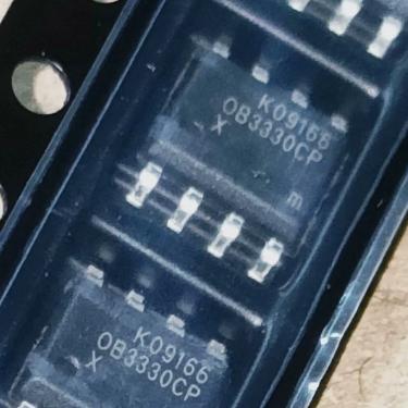

The OB3330XCPA operates as a primary-side regulated flyback LED controller with integrated power factor correction, using transition mode (boundary conduction mode) switching for high efficiency.

Primary-Side Regulation (PSR): Unlike conventional secondary-side regulated converters that require an optocoupler to feed back output voltage/current information across the isolation boundary, the OB3330X derives output current information from the primary side. During the MOSFET off-time, the transformer secondary current flows through the output diode to the LED load. This secondary current is reflected to the primary side as a voltage across the current sense resistor (RCS) at the CS pin. The peak primary current and the demagnetization time (measured by the ZCD pin) together determine the average output current. The internal error amplifier (gm amplifier) with reference voltage (400 mV typical) maintains constant output current regulation by adjusting the MOSFET peak current set point.

Power Factor Correction (PFC): The analog multiplier takes the rectified AC line voltage (sampled at the MULT pin from a voltage divider off the DC bus) and multiplies it with the error amplifier output (COMP pin). The multiplier output sets the peak current threshold for each switching cycle, forcing the input current envelope to follow the sinusoidal input voltage waveform. This achieves high power factor (PF > 0.9) without an additional PFC stage. The multiplier gain is 0.9 1/V (typical) with the MULT input linear range of 0 to 3V.

Transition Mode Operation: The ZCD (Zero Current Detection) pin monitors the auxiliary winding voltage. When the transformer is fully demagnetized (secondary current reaches zero), the auxiliary winding voltage drops, and the ZCD comparator detects this transition. After a minimum off-time of 3.5 us, the controller initiates the next switching cycle. This boundary conduction mode ensures the transformer resets completely before the next cycle, preventing transformer saturation and enabling near-zero-voltage switching (the MOSFET drain voltage rings to a valley before turn-on). The maximum off-time is 55 us; if no ZCD signal is detected within this period, the controller restarts a switching cycle.

Current Limiting: The CS pin senses the MOSFET source current through an external sense resistor. When the CS voltage exceeds the threshold set by the OCP_TH pin (selectable at 2.1V, 1.8V, or 1.5V), the gate drive is immediately turned off with a propagation delay of approximately 100 ns. The built-in 300 ns leading-edge blanking prevents false tripping from the turn-on current spike. The maximum on-time is limited to 50 us as an additional safety measure.

Output Over-Voltage Protection: The ZCD pin also monitors the auxiliary winding voltage during the MOSFET off-time. If the output voltage rises abnormally (e.g., LED open circuit), the reflected auxiliary voltage increases. When the ZCD voltage exceeds the OVP threshold of 3.75-4.25V (typical 4V), the controller shuts down and enters a restart cycle.

VCC Supply: The VCC pin is powered from the auxiliary winding through a rectifier diode and filter capacitor. During startup, the VCC is charged by the internal high-voltage start-up circuit (or an external start-up resistor) until it exceeds the UVLO off threshold (14.6V typical), at which point switching begins. If VCC drops below the UVLO on threshold (9V typical), switching stops and the controller re-enters the start-up mode. VCC over-voltage protection activates at 30V.

针脚 名称 类型 说明
1 ZCD 输入 Zero Current Detection; monitors auxiliary winding for transformer demagnetization; also used for output over-voltage protection; detection thresholds: demagnetization start 0.9V, end 0.3V, OVP 4V typical
2 OCP_TH 输入/输出 Over-current protection threshold setting; internal current source (17-39 uA) pulls up this pin through external resistor to set OCP threshold; thresholds: 2.1V (OCP_TH 1.5V)
3 MULT 输入 Multiplier input; connects to voltage divider from rectified DC bus for PFC; linear operating range 0-3V; determines peak current envelope shape to follow AC input waveform
4 COMP 输入/输出 Loop compensation; connects to external RC compensation network for error amplifier stability; dynamic range 1.2V-6V; transconductance 80 uS; DC gain 60-70 dB
5 CS 输入 Current sense input; connects to MOSFET source sense resistor; built-in 300 ns leading-edge blanking; OCP propagation delay 100 ns; compared against OCP threshold
6 接地 电源 Ground; connect to power ground plane
7 GATE 输出 Gate drive output; totem-pole driver for external N-channel MOSFET; rise time 80-150 ns, fall time 30-70 ns at CL=1nF; output clamped at 11-12.5V (VCC=28V) for gate protection
8 VCC 电源 Power supply input; UVLO on: 9V (typ), UVLO off: 14.6V (typ); OVP: 30V; clamp: 32V; start-up current: 5-15 uA; operating current: 1.5-2.5 mA (no switching); bypass with 0.1uF + 10uF to GND
应用 说明
Industrial LED Lighting High-bay, warehouse, and factory LED luminaires; 85-265VAC universal input; PF>0.9 meets industrial lighting regulations; PSR eliminates optocoupler for higher reliability in harsh environments
Commercial LED Lighting Panel lights, downlights, and troffers; constant current output drives LED strings directly; single-stage PFC reduces component count and PCB area; high efficiency reduces thermal management requirements
Residential LED Lighting LED bulb drivers and residential fixtures; low BOM count reduces system cost; comprehensive protection features ensure safe operation; compact SOP-8 package fits small driver enclosures
LED Driver Power Supply Isolated flyback converter for LED power supplies; transition mode operation achieves high efficiency; selectable OCP threshold accommodates different power levels; soft-start prevents output overshoot
Battery-Powered LED Systems Low standby current and start-up current minimize no-load power consumption; wide VCC operating range supports various auxiliary winding designs; over-temperature protection ensures safe operation in sealed enclosures
模型 制造商 兼容性 主要区别
OB3330CP 亮灯 功能相同 Same silicon; tube packaging instead of tape and reel; different ordering suffix; same SOP-8 package and electrical specifications
BP3371 BP Semiconductor 功能相似 High PF PSR LED driver; similar single-stage PFC flyback topology; SOP-8 package; check pin compatibility before PCB re-use
SY50283F Silergy 功能相似 Primary-side regulation LED driver; high PF; different pinout; similar application scope; verify OCP and protection features match requirements
OB3350CP 亮灯 功能相似 Cost-effective LED controller; no PFC function; simpler design for non-PF-critical applications; same manufacturer; different feature set
MP4027GS MPS 功能相似 Primary-side controlled LED driver with PFC; SOIC-8 package; different internal architecture; comparable performance specifications
推荐部件
质量保证

我们从合作供应链采购的所有电子元件都经过严格的进货检验。通过仔细的测试,我们确保交付给客户的所有产品都是原装正品,符合质量要求。此外,我们还保存完整的检验记录,使整个供应链流程清晰可查。.

认证
我们获得了多项专业认证,并建立了自己的专业检测实验室,确保交付给客户的每一件产品都符合最高质量要求。我们严格按照流程进行检测,确保产品质量稳定、参数准确。为保证原装正品,我们还与可靠的第三方检测机构合作,进行严格的质量检测。我们始终高度重视质量,完全符合行业标准、相关法规和 ISO 9001:2015 的要求。.

发货与付款

我们从合作供应链采购的所有电子元件都经过严格的进货检验。通过仔细的测试,我们确保交付给客户的所有产品都是原装正品,符合质量要求。此外,我们还保存完整的检验记录,使整个供应链流程清晰可查。.

认证
我们获得了多项专业认证,并建立了自己的专业检测实验室,确保交付给客户的每一件产品都符合最高质量要求。我们严格按照流程进行检测,确保产品质量稳定、参数准确。为保证原装正品,我们还与可靠的第三方检测机构合作,进行严格的质量检测。我们始终高度重视质量,完全符合行业标准、相关法规和 ISO 9001:2015 的要求。.

服务与包装

我们从合作供应链采购的所有电子元件都经过严格的进货检验。通过仔细的测试,我们确保交付给客户的所有产品都是原装正品,符合质量要求。此外,我们还保存完整的检验记录,使整个供应链流程清晰可查。.

认证
我们获得了多项专业认证,并建立了自己的专业检测实验室,确保交付给客户的每一件产品都符合最高质量要求。我们严格按照流程进行检测,确保产品质量稳定、参数准确。为保证原装正品,我们还与可靠的第三方检测机构合作,进行严格的质量检测。我们始终高度重视质量,完全符合行业标准、相关法规和 ISO 9001:2015 的要求。.



