首页 > 集成电路 IC > MMBT3904LT1G

MMBT3904LT1G


200 mA、40 V NPN 通用 BJT,SOT-23 封装,300 MHz fT,AEC-Q101,3000 卷装

1746768

有效库存
转到查询

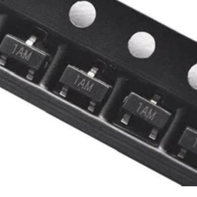
Image for reference only

制造商零件:

MMBT3904LT1G

包装:

SOT-23-3(2.9 x 1.3 毫米)

品牌:
产品类别:
您可能感兴趣的其他建议.
说明

The MMBT3904LT1G is a 200 mA, 40 V NPN general-purpose bipolar junction transistor from onsemi in a SOT-23-3 surface-mount package. It features a DC current gain (hFE) of 100-300 at 10 mA, transition frequency of 300 MHz, VCE(sat) of 0.2 V max at 10 mA, and 225 mW power dissipation. The device is AEC-Q101 qualified, Pb-free, halogen-free, and RoHS compliant, operating from -55°C to +150°C. Packaged in a 3,000-unit tape and reel with MSL-1 rating and top mark “1AM”, it is the industry-standard SMD equivalent of the 2N3904.

The MMBT3904LT1G is a 200 mA, 40 V NPN general-purpose bipolar junction transistor manufactured by onsemi, housed in the industry-standard SOT-23-3 (TO-236) surface-mount package. It is the SMD equivalent of the classic 2N3904 through-hole transistor and is one of the most widely used small-signal NPN transistors in electronics.

Key specifications include a collector-emitter breakdown voltage (VCEO) of 40 V, collector-base voltage (VCBO) of 60 V, emitter-base voltage (VEBO) of 6 V, and continuous collector current of 200 mA. The device achieves a DC current gain (hFE) ranging from 40 to 300 depending on operating point (100 minimum at IC = 10 mA, VCE = 1 V), collector-emitter saturation voltage (VCE(sat)) of 0.2 V maximum at IC = 10 mA, and transition frequency (fT) of 300 MHz minimum. Output capacitance (Cobo) is 4.0 pF and input capacitance (Cibo) is 8.0 pF.

Switching characteristics include delay time of 35 ns, rise time of 35 ns, storage time of 200 ns, and fall time of 50 ns. Total power dissipation is 225 mW on FR-5 board with thermal resistance of 556°C/W (junction-to-ambient). The device operates over a junction temperature range of -55°C to +150°C.

The MMBT3904LT1G is Pb-free, halogen-free/BFR-free, RoHS compliant, and AEC-Q101 qualified with PPAP capability. The LT1G suffix denotes tape and reel packaging with 3,000 units per reel. MSL-1 rated (unlimited floor life). The top mark is typically “1AM”.

The MMBT3904LT1G operates as an NPN bipolar junction transistor (BJT), using current-controlled current amplification to switch or amplify signals.

Active Mode: When the base-emitter junction is forward-biased (VBE > 0.65 V typical) and the base-collector junction is reverse-biased, the transistor operates in the active region. A small base current (IB) controls a much larger collector current (IC) through current gain (hFE = IC/IB). With hFE ranging from 40 to 300, the MMBT3904LT1G can amplify small signals or drive moderate loads with minimal base drive.

Saturation Mode: When both junctions are forward-biased (VCE drops to VCE(sat) ≈ 0.2 V), the transistor is fully on, acting as a closed switch between collector and emitter. The low saturation voltage minimizes power dissipation in switching applications. To ensure hard saturation, the base current should exceed IC/hFE by a factor of 2-10 (overdrive factor).

Cutoff Mode: With the base-emitter junction reverse-biased or at zero bias, both junctions are reverse-biased and only tiny leakage currents flow (ICEX < 50 nA). The transistor acts as an open switch.

Switching Behavior: Transition between cutoff and saturation is governed by charge storage in the base region. Turn-on delay (35 ns) and rise time (35 ns) are fast due to rapid charge injection. Turn-off involves removing stored base charge, with storage time (200 ns) dominating the total turn-off period. Fall time is 50 ns. The 300 MHz transition frequency indicates the gain-bandwidth product, beyond which current gain drops below unity.

Small-Signal Operation: In the active region, the transistor presents an input impedance (hie) of 1.0-10 kΩ, voltage feedback ratio (hre) of 0.5-8.0 × 10⁻⁴, small-signal current gain (hfe) of 100-400, and output admittance (hoe) of 1.0-40 μmhos at IC = 1 mA. These parameters make it suitable for low-frequency amplification stages.

Thermal Behavior: The VBE temperature coefficient is approximately -2 mV/°C, meaning the base-emitter voltage decreases with rising temperature. This characteristic must be accounted for in bias circuit design to maintain stable operating points across temperature.

针脚 名称 类型 默认功能 说明
1 发射器 G Emitter Terminal Current flows out of the emitter; typically connected to ground in common-emitter configuration
2 基地 I Base Control Input Current-controlled input; small base current modulates larger collector current; forward bias VBE ≈ 0.65 V
3 收藏家 O Collector Terminal Current flows into the collector; connects to load resistor or driven load in switching applications
应用 说明
Logic-Level Signal Switching General-purpose switching of LEDs, relays, buzzers, and other low-current loads driven from 3.3V or 5V microcontroller GPIO pins
Small-Signal Amplification Low-frequency preamplifier stages in audio, sensor conditioning, and instrumentation circuits where moderate gain and low noise are required
Level Shifting Translating logic signals between different voltage domains (e.g., 3.3V to 5V) using common-emitter or common-collector configurations
Driver Circuits Base driver for power transistors or MOSFET gate drivers in multi-stage switching circuits
汽车电子 AEC-Q101 qualified for sensor signal conditioning, indicator driving, and general switching in automotive body electronics
模型 制造商 兼容性 主要区别
MMBT3904LT3G onsemi 引脚兼容/电气相同 Same die and specs; 10,000-unit reel instead of 3,000; preferred for high-volume production
MMBT3904-7-F 二极管公司 针脚兼容 Same electrical specs from different manufacturer; slight differences in hFE binning and marking code
BC847C Nexperia 针脚兼容 45V, 100 mA, hFE = 420-800 (higher gain); lower current rating, different gain range
MMBT2222ALT1G onsemi 针脚兼容 40V, 600 mA (higher current), 300 MHz; higher current capability for driving heavier loads
2N3904 各种 Electrically Equivalent Through-hole TO-92 version; same transistor in leaded package for prototyping and hand assembly
推荐部件
Single 2-input OR gate, UHS TinyLogic, 1.65-5.5V, 2.4ns, SOT-23-5

品牌:

封装:

SOT-23-5 (3.0 x 1.5 x 0.95 mm)
有库存:
15000 件

货运周期:3~7 天
最低订购量为 1

转到查询
P-Channel MOSFET, -50V, -130mA, 10 Ohm RDS(on), SOT-23, logic level

品牌:

封装:

SOT-23-3 (2.9 x 1.3 x 1.0 mm)
有库存:
4891pcs

货运周期:3~7 天
最低订购量为 1

转到查询
1.5W 18V Zener diode, SMA package, 5% tolerance, AEC-Q101, ESD Class 3

品牌:

封装:

SMA (DO-214AC) (4.32 x 2.6 x 2.0 mm)
有库存:
7948pcs

货运周期:3~7 天
最低订购量为 1

转到查询
1A, 1000V standard recovery rectifier, SMA package, glass passivated

品牌:

封装:

SMA (DO-214AC), 2.60 x 5.10 x 1.00 mm
有库存:
2409 件

货运周期:3~7 天
最低订购量为 1

转到查询
3-pin uP reset monitor, push-pull RESET, 4.63V threshold, SOT-23

品牌:

封装:

SOT-23-3
有库存:
3824 件

货运周期:3~7 天
最低订购量为 1

转到查询
Dual bipolar op-amp, 4.5MHz GBW, 13V/μs slew, 3-44V single supply, SOIC-8

品牌:

封装:

SOIC-8 (3.9 x 4.9 x 1.5mm)
有库存:
3480pcs

货运周期:3~7 天
最低订购量为 1

转到查询
质量保证

我们从合作供应链采购的所有电子元件都经过严格的进货检验。通过仔细的测试,我们确保交付给客户的所有产品都是原装正品,符合质量要求。此外,我们还保存完整的检验记录,使整个供应链流程清晰可查。.

认证
我们获得了多项专业认证,并建立了自己的专业检测实验室,确保交付给客户的每一件产品都符合最高质量要求。我们严格按照流程进行检测,确保产品质量稳定、参数准确。为保证原装正品,我们还与可靠的第三方检测机构合作,进行严格的质量检测。我们始终高度重视质量,完全符合行业标准、相关法规和 ISO 9001:2015 的要求。.

发货与付款

我们从合作供应链采购的所有电子元件都经过严格的进货检验。通过仔细的测试,我们确保交付给客户的所有产品都是原装正品,符合质量要求。此外,我们还保存完整的检验记录,使整个供应链流程清晰可查。.

认证
我们获得了多项专业认证,并建立了自己的专业检测实验室,确保交付给客户的每一件产品都符合最高质量要求。我们严格按照流程进行检测,确保产品质量稳定、参数准确。为保证原装正品,我们还与可靠的第三方检测机构合作,进行严格的质量检测。我们始终高度重视质量,完全符合行业标准、相关法规和 ISO 9001:2015 的要求。.

服务与包装

我们从合作供应链采购的所有电子元件都经过严格的进货检验。通过仔细的测试,我们确保交付给客户的所有产品都是原装正品,符合质量要求。此外,我们还保存完整的检验记录,使整个供应链流程清晰可查。.

认证
我们获得了多项专业认证,并建立了自己的专业检测实验室,确保交付给客户的每一件产品都符合最高质量要求。我们严格按照流程进行检测,确保产品质量稳定、参数准确。为保证原装正品,我们还与可靠的第三方检测机构合作,进行严格的质量检测。我们始终高度重视质量,完全符合行业标准、相关法规和 ISO 9001:2015 的要求。.



