首页 > 集成电路 IC > MAX232DR

MAX232DR


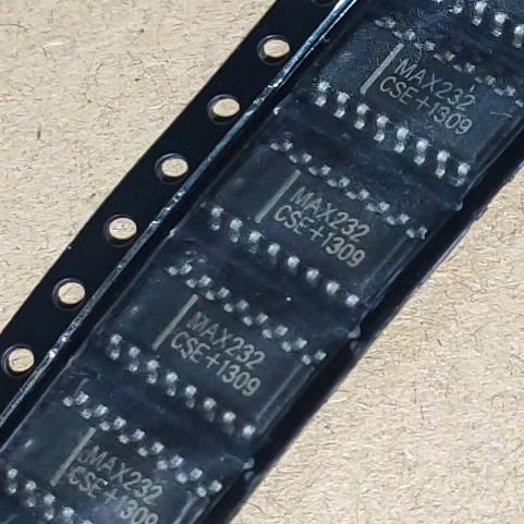
Dual RS-232 driver/receiver, 2TX/2RX, 120kbps, 5V single supply, charge pump, SOIC-16, 0~70C

24465

有效库存
转到查询

Image for reference only

制造商零件:

MAX232DR

包装:

SOIC-16 (9.9 x 3.91 x 1.58 mm)

品牌:
您可能感兴趣的其他建议.
说明

The MAX232DR from Texas Instruments is a dual RS-232 driver/receiver in SOIC-16 package that operates from a single 5V supply using integrated charge pump circuitry to generate TIA/EIA-232-F voltage levels. The device includes two drivers and two receivers, supporting data rates up to 120 kbps with full-duplex operation. Each driver converts TTL/CMOS input levels to TIA/EIA-232-F levels (typical output swing plus/minus 9V), and each receiver converts RS-232 inputs to 5V TTL/CMOS levels with 1.3V typical threshold and 0.5V hysteresis. Receivers accept up to plus/minus 30V input levels. The charge pump requires only four external 1uF capacitors. Typical supply current: 8mA. ESD protection exceeds 2kV HBM per JESD 22. Operating temperature: 0C to 70C. Supply range: 4.5V to 5.5V. MSL-1, RoHS3, EAR99. Tape and reel, 2500/reel.

The MAX232DR from Texas Instruments is a dual RS-232 driver/receiver housed in a 16-pin SOIC package, operating from a single 5V supply with integrated capacitive charge pump circuitry that generates the TIA/EIA-232-F voltage levels (typically plus/minus 9V output) without requiring external dual supplies.

The device contains two independent drivers and two independent receivers, providing full-duplex communication capability at data rates up to 120 kbps. Each driver converts TTL/CMOS logic levels (0 to 5V) into RS-232 compliant voltage levels, while each receiver converts RS-232 input levels into TTL/CMOS compatible outputs. The receivers feature a typical threshold of 1.3V with 0.5V hysteresis for noise immunity, and can accept input voltages up to plus/minus 30V.

The internal charge pump uses a voltage doubler and voltage inverter, requiring only four external 1uF capacitors (C1+, C1-, C2+, C2-) to generate the plus and minus supplies needed for RS-232 output levels. The V+ pin (pin 2) outputs approximately 2xVCC (about 10V), and the V- pin (pin 6) outputs approximately -2xVCC (about -10V). These generated voltages are used internally by the drivers and should not be used to power external circuits beyond a small bypass capacitor.

The MAX232DR is one of the most widely used RS-232 interface ICs in the electronics industry, found in virtually every device that requires serial communication via RS-232. The DR suffix denotes SOIC-16 package with tape and reel packaging (2,500 units per reel). The device is RoHS3 compliant, MSL Level 1 (unlimited), and classified as EAR99. Note that TI lists MAX232D as discontinued, with MAX232DR as the recommended replacement with plus/minus 2kV ESD protection.

The MAX232DR operates as a dual-channel RS-232 level translator, converting between TTL/CMOS logic levels (0-5V) and TIA/EIA-232-F voltage levels (plus/minus 5V to plus/minus 15V) using an integrated charge pump to generate the required high-voltage rails from a single 5V supply.

Charge Pump Operation: The internal charge pump consists of two stages. The first stage is a voltage doubler that uses an external capacitor (C1) to double the VCC supply, producing approximately 2xVCC (about 10V) at the V+ output (pin 2). The second stage is a voltage inverter that uses another external capacitor (C2) to invert the V+ voltage, producing approximately -2xVCC (about -10V) at the V- output (pin 6). Two additional external capacitors (C3, C4) serve as energy storage for the V+ and V- rails respectively. All four capacitors are typically 1uF (non-polarized ceramic recommended). During each charge pump cycle, the internal oscillator alternately charges and transfers charge between the capacitors, maintaining the V+ and V- supplies at the required levels for RS-232 output compliance.

Driver Operation: Each driver takes a TTL/CMOS logic input (T1IN or T2IN) and converts it to an RS-232 compliant output (T1OUT or T2OUT). When the input is logic HIGH (greater than 2.4V), the output swings toward V- (typically -8.5V). When the input is logic LOW (less than 0.8V), the output swings toward V+ (typically +8.5V). Note that the driver inverts the signal: a HIGH TTL input produces a negative RS-232 voltage (mark), and a LOW TTL input produces a positive RS-232 voltage (space), which is the correct polarity for RS-232 communication. The driver output impedance is typically 300 ohms, and the output is current-limited for short-circuit protection.

Receiver Operation: Each receiver takes an RS-232 input (R1IN or R2IN) and converts it to a TTL/CMOS logic output (R1OUT or R2OUT). The receiver has a switching threshold of approximately 1.3V with 0.5V hysteresis. Input voltages above the threshold are interpreted as logic LOW on the output (inverted), while input voltages below the threshold are interpreted as logic HIGH. The hysteresis provides noise immunity against signal reflections and ground potential differences common in RS-232 cables. The receiver inputs can accept plus/minus 30V without damage, providing robust protection against voltage spikes common in long cable runs.

Signal Flow in Typical Application: The UART TXD output (TTL) connects to T1IN; T1OUT drives the RS-232 cable (DB9 pin 3). The RS-232 cable (DB9 pin 2) connects to R1IN; R1OUT drives the UART RXD input (TTL). This provides bidirectional level translation between the microcontroller and the RS-232 serial port.

针脚 名称 类型 说明
1 C1+ Passive Positive terminal of charge pump capacitor C1; connect to pin 3 (C1-) through 1uF capacitor
2 V+ 输出 Positive charge pump output; approximately +2xVCC (about +10V); for storage capacitor only, do not use as external supply
3 C1- Passive Negative terminal of charge pump capacitor C1; connect to pin 1 (C1+) through 1uF capacitor
4 C2+ Passive Positive terminal of charge pump capacitor C2; connect to pin 5 (C2-) through 1uF capacitor
5 C2- Passive Negative terminal of charge pump capacitor C2; connect to pin 4 (C2+) through 1uF capacitor
6 V- 输出 Negative charge pump output; approximately -2xVCC (about -10V); for storage capacitor only
7 T2OUT 输出 Driver 2 RS-232 output; connects to remote RS-232 system; swings between V+ and V-
8 R2IN 输入 Receiver 2 RS-232 input; from remote RS-232 system; accepts up to plus/minus 30V
9 R2OUT 输出 Receiver 2 TTL/CMOS output; to UART RXD; inverts RS-232 input polarity
10 T2IN 输入 Driver 2 TTL/CMOS input; from UART TXD; inverts to RS-232 output
11 T1IN 输入 Driver 1 TTL/CMOS input; from UART TXD; logic HIGH produces negative RS-232 output
12 R1OUT 输出 Receiver 1 TTL/CMOS output; to UART RXD; 1.3V threshold with 0.5V hysteresis
13 R1IN 输入 Receiver 1 RS-232 input; from remote RS-232 system; accepts up to plus/minus 30V
14 T1OUT 输出 Driver 1 RS-232 output; connects to DB9 pin 3 (TXD); swings between V+ and V-
15 接地 电源 接地;连接至系统地平面
16 VCC 电源 Supply voltage; 4.5V to 5.5V; bypass with 0.1uF ceramic capacitor to GND
应用 说明
UART Serial Communication Level translation between MCU UART (TTL 0-5V) and RS-232 serial port (plus/minus 12V); single 5V supply eliminates need for external dual-rail power
Industrial Serial Interfaces RS-232 communication in industrial equipment, PLCs, and CNC machines; plus/minus 30V receiver input tolerance withstands noise in factory environments
Debug/Programming Ports Console and debug serial ports on embedded systems; RS-232 level conversion for development boards and evaluation modules
Modems and Terminals TIA/EIA-232-F compliant interface for legacy modems, terminals, and peripherals; 120kbps data rate supports standard serial communication speeds
Battery-Powered Systems Low 8mA typical supply current; single 5V operation; charge pump eliminates bulky dual-rail power supplies in portable equipment
模型 制造商 兼容性 主要区别
MAX202DR TI 针脚兼容 Enhanced ESD protection (15kV HBM vs 2kV); uses 0.1uF charge pump caps instead of 1uF; same SOIC-16 pinout
MAX3232DR TI 功能相似 3.3V supply version; wider voltage range (3.0-5.5V); 250kbps data rate; different charge pump cap values
ST3232DR ST 针脚兼容 3.0-5.5V supply range; 250kbps; STMicro equivalent; check ESD specs for critical applications
SP3232EEN MaxLinear 针脚兼容 3.3V RS-232 transceiver; 250kbps; plus/minus 15kV ESD HBM; SOIC-16
ADM3202ARNZ ADI 针脚兼容 3.3V dual RS-232 transceiver; 460kbps data rate; 0.1uF charge pump caps; SOIC-16
推荐部件
3-16S battery monitor/protector, Li-Ion/LiFePO4, 2 ADCs, TQFP-48

品牌:

封装:

TQFP-48 (7 x 7 x 1.0 mm)
有库存:
2150pcs

货运周期:3~7 天
最低订购量为 1

转到查询
I2C 4.5A 1-cell Li-ion charger, NVDC power path, USB OTG, VQFN-24

品牌:

封装:

VQFN-24 (4.0 x 4.0 x 0.75 mm, with thermal pad)
有库存:
4182pcs

货运周期:3~7 天
最低订购量为 1

转到查询
Single micropower RRIO op-amp, 2.7-10V, 65kHz, 11uA, SOT-23-5

品牌:

封装:

SOT-23-5 (2.9 x 2.8 x 1.15 mm)
有库存:
8750pcs

货运周期:3~7 天
最低订购量为 1

转到查询
Single 2-input AND gate, 1.65-5.5V, 24mA drive, SOT-23-5, LVC

品牌:

封装:

SOT-23-5 (2.9 x 1.6 x 1.15 mm)
有库存:
35000 件

货运周期:3~7 天
最低订购量为 1

转到查询
8-bit parallel-load shift register, PISO, 2-6V, 24 MHz, SOIC-16

品牌:

封装:

SOIC-16 (9.9 x 6.0 mm)
有库存:
4837pcs

货运周期:3~7 天
最低订购量为 1

转到查询
Quad differential line receiver, EIA-422/423, 3-state TTL outputs, 5V, SOIC-16

品牌:

封装:

SOIC-16 (9.9 x 6.0 mm)
有库存:
0 件

货运周期:3~7 天
最低订购量为 1

转到查询
质量保证

我们从合作供应链采购的所有电子元件都经过严格的进货检验。通过仔细的测试,我们确保交付给客户的所有产品都是原装正品,符合质量要求。此外,我们还保存完整的检验记录,使整个供应链流程清晰可查。.

认证
我们获得了多项专业认证,并建立了自己的专业检测实验室,确保交付给客户的每一件产品都符合最高质量要求。我们严格按照流程进行检测,确保产品质量稳定、参数准确。为保证原装正品,我们还与可靠的第三方检测机构合作,进行严格的质量检测。我们始终高度重视质量,完全符合行业标准、相关法规和 ISO 9001:2015 的要求。.

发货与付款

我们从合作供应链采购的所有电子元件都经过严格的进货检验。通过仔细的测试,我们确保交付给客户的所有产品都是原装正品,符合质量要求。此外,我们还保存完整的检验记录,使整个供应链流程清晰可查。.

认证
我们获得了多项专业认证,并建立了自己的专业检测实验室,确保交付给客户的每一件产品都符合最高质量要求。我们严格按照流程进行检测,确保产品质量稳定、参数准确。为保证原装正品,我们还与可靠的第三方检测机构合作,进行严格的质量检测。我们始终高度重视质量,完全符合行业标准、相关法规和 ISO 9001:2015 的要求。.

服务与包装

我们从合作供应链采购的所有电子元件都经过严格的进货检验。通过仔细的测试,我们确保交付给客户的所有产品都是原装正品,符合质量要求。此外,我们还保存完整的检验记录,使整个供应链流程清晰可查。.

认证
我们获得了多项专业认证,并建立了自己的专业检测实验室,确保交付给客户的每一件产品都符合最高质量要求。我们严格按照流程进行检测,确保产品质量稳定、参数准确。为保证原装正品,我们还与可靠的第三方检测机构合作,进行严格的质量检测。我们始终高度重视质量,完全符合行业标准、相关法规和 ISO 9001:2015 的要求。.



