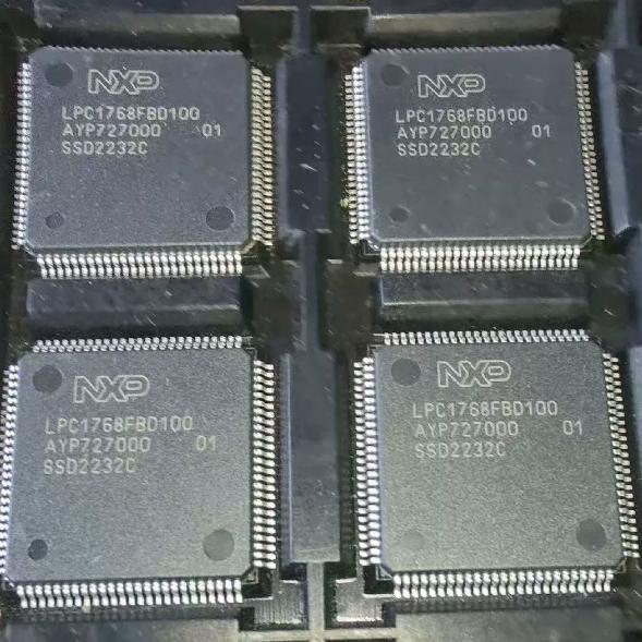
LPC1768FBD100


ARM Cortex-M3 MCU 100MHz, 512KB Flash, 64KB SRAM, Ethernet, USB 2.0 FS Host/Dev/OTG, 2x CAN, 4x UART, 8ch DMA, ADC, DAC, motor PWM, LQFP-100, -40~85C

6000

Effective Inventory
Go to Inquiry

Image for reference only

Manufacturer Part:

LPC1768FBD100

Package:

LQFP-100 (SOT407-1) (14 x 14 x 1.4 mm, 0.5mm pitch)

Brand:
Other recommendations you may be interested in.
Description

The LPC1768FBD100 from NXP Semiconductors is an ARM Cortex-M3 based 32-bit microcontroller featuring 512 KB Flash memory, 64 KB SRAM, and a comprehensive peripheral set in a 100-pin LQFP (14 x 14 x 1.4 mm) package. Key specifications: ARM Cortex-M3 core at up to 100 MHz with 3-stage pipeline, Harvard architecture, and internal prefetch unit; 512 KB on-chip Flash with ISP and IAP support; 64 KB on-chip SRAM; Memory Protection Unit (MPU) with 8 regions; 8-channel General Purpose DMA controller (GPDMA) on AHB multilayer matrix; Ethernet MAC with RMII interface and dedicated DMA; USB 2.0 full-speed Device/Host/OTG controller with on-chip PHY and dedicated DMA; 4 UARTs with fractional baud rate generation, internal FIFO, and DMA support (one with modem control and RS-485, one with IrDA); 2-channel CAN 2.0B controller; 1 SPI controller with programmable data length; 2 SSP controllers with FIFO and multi-protocol support; 3 enhanced I2C bus interfaces (one supports Fast Mode Plus at 1 Mbit/s); I2S interface with fractional rate control and DMA; 70 GPIO pins with configurable pull-up/down resistors and open-drain mode; 12-bit 8-channel ADC with up to 200 kHz conversion rate; 10-bit DAC with dedicated timer and DMA; 4 general purpose 32-bit timers/counters; motor control PWM supporting 3-phase motor control; quadrature encoder interface; 6-output general purpose PWM; ultra-low power RTC with separate battery supply (VBAT pin) and dedicated oscillator; watchdog timer (WDT); system tick timer with external clock option; repetitive interrupt timer; 4 reduced power modes (Sleep, Deep-sleep, Power-down, Deep power-down); Wake-up Interrupt Controller (WIC); brownout detect with separate interrupt and reset thresholds; power-on reset (POR); crystal oscillator 1-25 MHz; 4 MHz internal RC oscillator trimmed to 1 percent; PLL for CPU and USB clocks; code read protection (CRP) with multiple security levels; unique device serial number; single 3.3 V supply (2.4 V to 3.6 V); 4 external interrupt inputs configurable as edge/level sensitive; NMI input; operating temperature -40 to +85 degrees C; RoHS compliant; pin-compatible with LPC2368 ARM7 MCU. Active status.

The LPC1768FBD100 from NXP Semiconductors is the flagship member of the LPC176x/5x family of ARM Cortex-M3 microcontrollers, offering the maximum memory density (512 KB Flash / 64 KB SRAM) and the full peripheral set in a 100-pin LQFP package. It is one of the most popular and widely-deployed Cortex-M3 MCUs in the industry, with a mature ecosystem and extensive software support.

The LPC1768 is significant because it was one of the first Cortex-M3 devices to integrate Ethernet MAC, USB 2.0, and CAN in a single chip, targeting industrial networking, motor control, and smart metering applications that previously required multiple chips or a higher-end ARM9 processor. The pin-compatibility with the older LPC2368 (ARM7TDMI) allows easy migration from ARM7 to Cortex-M3 with only software changes.

The ARM Cortex-M3 core runs at up to 100 MHz and achieves 1.25 DMIPS/MHz (125 DMIPS at 100 MHz). The 3-stage pipeline with speculative branch prefetch provides efficient instruction throughput. The built-in NVIC supports up to 33 interrupt vectors with 8 programmable priority levels, enabling deterministic real-time interrupt handling. The MPU allows privileged software to define 8 memory regions with individual access permissions, protecting critical data from corruption by unprivileged code.

The 512 KB Flash provides ample code storage for complex applications including TCP/IP stacks, USB device stacks, CAN protocol stacks, and motor control algorithms. The Flash supports in-system programming (ISP) via UART and in-application programming (IAP) for firmware updates, data logging, and boot loader implementation. The 64 KB SRAM is sufficient for large application data structures, network buffers, and USB endpoint buffers.

The 8-channel GPDMA is a key performance feature that allows data transfers between peripherals and memory without CPU intervention. Each DMA channel can be triggered by UART, SSP, I2S, ADC, DAC, timer match events, or external DMA requests. The multilayer AHB matrix provides separate bus paths for the CPU, DMA, Ethernet, and USB, eliminating arbitration delays and allowing concurrent bus transactions. This architecture enables the CPU to execute code from Flash while the DMA simultaneously transfers Ethernet packets and USB data.

The Ethernet MAC with RMII interface and dedicated DMA controller provides full 10/100 Mbps Ethernet capability. The MAC implements the IEEE 802.3 MAC layer including CRC generation/checking, frame filtering, and flow control. The dedicated DMA engine handles frame reception and transmission autonomously, reducing CPU overhead for network communication. An external PHY chip (such as DP83848 or LAN8720) is required to complete the physical layer.

The USB 2.0 full-speed controller supports Device, Host, and OTG modes. In Device mode, it supports up to 16 endpoints (in addition to EP0) with dedicated DMA. In Host mode, it can enumerate and communicate with USB peripherals. The OTG mode allows the device to act as either host or peripheral. The on-chip PHY eliminates the need for an external USB transceiver.

The dual CAN 2.0B controller is essential for automotive and industrial applications. Each channel supports standard (11-bit) and extended (29-bit) identifiers, with individual acceptance filters. The CAN controller handles bit timing, stuffing, CRC, and error management in hardware, reducing CPU overhead.

The motor control PWM supports 3-phase motor drive with complementary PWM outputs, dead-time generation, and fault protection inputs. Combined with the ADC (which can be synchronized to the PWM for current sampling) and the quadrature encoder interface, the LPC1768 provides a complete motor control subsystem.

The 4 low-power modes (Sleep, Deep-sleep, Power-down, Deep power-down) with the Wake-up Interrupt Controller (WIC) enable battery-powered applications. In Deep power-down mode, the RTC can remain operational from the VBAT supply while the rest of the chip is powered down, consuming only a few microamps.

The mbed platform (now part of Arm) originally launched with the LPC1768 as its reference MCU, and the mbed online compiler and HDK were designed around it. This gives the LPC1768 one of the largest collections of open-source libraries and example code among Cortex-M3 devices. The device is also supported by NXP’s MCUXpresso IDE, Keil MDK, IAR Embedded Workbench, and GCC-based toolchains.

The LPC1768FBD100 operates as a complete 32-bit embedded microcontroller system centered on the ARM Cortex-M3 processor core with a multilayer AHB bus matrix providing high-bandwidth data paths between masters and slaves.

ARM Cortex-M3 Core: The Cortex-M3 is a 32-bit RISC processor implementing the ARMv7-M architecture with the Thumb-2 instruction set. Unlike the older ARM7TDMI (which uses the ARM/Thumb instruction sets), the Cortex-M3 exclusively uses the mixed 16/32-bit Thumb-2 instruction set, achieving higher code density. The 3-stage pipeline (Fetch, Decode, Execute) with branch speculation provides single-cycle execution for most 16-bit instructions. The processor includes a hardware divide instruction (2-12 cycles), bit-band support for atomic bit manipulation, and unaligned memory access support.

NVIC and Interrupt Handling: The Nested Vectored Interrupt Controller supports up to 33 interrupt vectors with 8 priority levels. On interrupt, the processor automatically pushes 8 registers (R0-R3, R12, LR, PC, xPSR) to the stack in 12 cycles, and automatically pops them on return in 12 cycles. This tail-chaining and late-arrival optimization ensures deterministic interrupt latency. The WIC (Wake-up Interrupt Controller) allows the processor to wake from Deep-sleep and Power-down modes on any enabled interrupt without CPU intervention.

Multilayer AHB Matrix: The bus matrix provides 4 separate AHB buses for the 4 bus masters: CPU, DMA, Ethernet, and USB. Each master can access any slave (Flash, SRAM, peripheral registers) independently, without stalling other masters. The split APB bus allows the CPU and DMA to access different APB peripherals simultaneously. This architecture is critical for the Ethernet and USB DMA controllers to sustain high-throughput data transfers without impacting CPU execution.

Memory Map: The Cortex-M3 defines a fixed memory map. The Flash is mapped at 0x00000000 (code space), SRAM at 0x10000000 (data space), and peripherals at 0x40000000 (APB) and 0x50000000 (AHB). The bit-band region maps each bit in the 0x20000000 (SRAM) and 0x40000000 (peripheral) regions to a word address in the bit-band alias region, enabling atomic bit set/clear operations without read-modify-write sequences.

Clock System: The main oscillator (1-25 MHz external crystal) or the 4 MHz internal RC oscillator feeds the PLL0 which multiplies the frequency to generate the CPU clock (up to 100 MHz), the USB clock (48 MHz from PLL1), and the peripheral clocks. Each peripheral has its own clock divider, allowing unused peripherals to be clocked slowly or not at all to save power. The clock output function (CLKOUT) can reflect any internal clock on an external pin for debugging.

Power Management: The 4 power modes reduce power consumption progressively. Sleep mode stops the CPU clock but keeps all peripherals running; any interrupt wakes the CPU. Deep-sleep mode stops the Flash and most clocks; only the RTC, WDT, and BOD can generate wake-up interrupts. Power-down mode stops all internal clocks and the Flash; the WIC remains active and can wake the processor from external interrupts, RTC, USB activity, Ethernet wake-up, or CAN activity. Deep power-down mode turns off the entire chip except the RTC (powered from VBAT) and the WIC; current consumption is approximately 0.3 uA. The integrated PMU manages the power mode transitions automatically.

DMA Operation: The GPDMA supports 8 channels, each independently configurable for source/destination address, transfer size, burst size, and flow control. The DMA can perform memory-to-memory, memory-to-peripheral, and peripheral-to-memory transfers. Each peripheral that supports DMA (UART, SSP, I2S, ADC, DAC, timer match) has dedicated DMA request lines connected to the DMA controller. The DMA controller arbitrates between channels on a priority basis and generates an interrupt when a transfer completes or encounters an error.

Ethernet MAC: The MAC implements the IEEE 802.3 MAC layer with DMA. Received frames are stored in SRAM buffers pointed to by descriptor rings. The DMA engine manages the descriptor ring autonomously, fetching new descriptors and storing received data. Transmit frames are similarly described by descriptor rings. The MAC performs address filtering (promiscuous, hash, or exact match), VLAN tag detection, and frame checksum verification. The RMII interface connects to an external PHY chip with only 7 signals (REF_CLK, TXD[0:1], TX_EN, RXD[0:1], RX_ER, CRS_DV).

ADC and DAC: The 12-bit ADC uses a successive approximation register (SAR) architecture with a conversion time of approximately 2.4 us per channel at 200 kHz rate. The ADC can be triggered by timer match events for precise periodic sampling, or by the motor control PWM for synchronized motor current measurement. The 10-bit DAC uses an R-2R ladder network with a settling time of approximately 1 us. The DAC output can be synchronized to a timer for waveform generation, or driven by the DMA for arbitrary waveform output.

Pin Group Name Type Description
Power VDD(3V3), VDDA, VBAT, VSS, VSSA, VREFP, VREFN Power VDD(3V3): digital supply 2.4-3.6 V (multiple pins); VDDA: analog supply for ADC/DAC (must be connected through filtered path); VBAT: RTC battery backup supply (maintains RTC when main power is off); VSS/VSSA: ground/analog ground; VREFP/VREFN: ADC positive/negative reference (VREFN must equal VSSA); decouple each VDD with 100 nF + 10 uF; decouple VDDA with 100 nF + 10 uF with ferrite bead isolation from VDD
Clock XTAL1, XTAL2, RTCX1, RTCX2 Analog I/O XTAL1/XTAL2: main oscillator crystal pins (1-25 MHz); RTCX1/RTCX2: 32.768 kHz RTC crystal pins; connect crystal with load capacitors per crystal specification; can be left unconnected if using internal RC oscillator only
Reset RESET Input Active-low system reset; internal pull-up; asserting LOW generates system reset; connect 100 nF capacitor to GND for ESD filtering; open-drain output during reset for system-wide reset propagation
Debug TCK/SWDCLK, TMS/SWDIO, TDI, TDO, TRST Digital I/O Standard JTAG debug interface (5-pin); TCK/SWDCLK also serves as SWD clock; TMS/SWDIO also serves as SWD data; TDI and TRST are JTAG-only; SWD mode uses only 2 pins (SWDCLK, SWDIO); connect to debug probe (ULINK2, J-Link, CMSIS-DAP)
USB USB_D+, USB_D-, USB_CONNECT, VBUS Digital/Analog USB_D+/USB_D-: USB 2.0 full-speed differential data (on-chip PHY, direct connection to USB connector with 33 ohm series resistors); USB_CONNECT: USB soft-connect control (drives 1.5 kOhm pull-up on USB_D+); VBUS: USB VBUS detect input (sense USB bus power presence for OTG)
Ethernet ENET_TXD[0:1], ENET_RXD[0:1], ENET_TX_EN, ENET_RX_ER, ENET_CRS, ENET_REF_CLK, ENET_MDIO, ENET_MDC Digital RMII interface to external Ethernet PHY (7 signals); ENET_TXD/TX_EN: transmit data and enable; ENET_RXD/RX_ER/CRS/REF_CLK: receive data, error, carrier sense, and reference clock; ENET_MDIO/MDC: management data interface for PHY register access; connect directly to RMII PHY (DP83848, LAN8720, etc.)
CAN RD1, TD1, RD2, TD2 Digital CAN 2.0B bus receive and transmit pins for 2 channels; RD1/TD1: CAN channel 1; RD2/TD2: CAN channel 2; connect through external CAN transceiver (SN65HVD230, TJA1050, etc.); do not connect directly to CAN bus
GPIO Ports P0[0:31], P1[0:31], P2[0:31], P3[25:26], P4[28:29] I/O 70 GPIO pins with configurable pull-up/pull-down, open-drain mode, and alternate function selection; each pin has up to 5 alternate functions (UART, SPI, SSP, I2C, PWM, ADC, timer, etc.); pins are 3.6 V tolerant (not 5 V tolerant); alternate function selected via PINSEL registers
Analog AD0[0:7], AOUT, VREFP, VREFN Analog 8 ADC input channels (12-bit, up to 200 kHz); AOUT: 10-bit DAC output; VREFP/VREFN: ADC reference inputs; ADC channels share pins with GPIO (P0[23:30]); AOUT shares pin with P0[26]; separate analog supplies (VDDA, VSSA) minimize digital noise coupling
Application Description
Industrial Ethernet Gateway Use Ethernet MAC with external PHY for Modbus TCP, EtherNet/IP, or PROFINET communication; dual CAN for fieldbus interface; 512 KB Flash stores TCP/IP stack and application; 64 KB SRAM for network buffers; DMA handles Ethernet and CAN data autonomously; 4 UARTs connect to RS-232/RS-485 serial devices; ideal for protocol gateway converting between Ethernet and CAN/serial
3-Phase Motor Control Motor control PWM with complementary outputs drives 3-phase inverter; ADC synchronized to PWM samples motor phase currents; quadrature encoder interface reads motor position; 100 MHz CPU executes FOC algorithm in under 50 us; CAN interface connects to higher-level controller; RS-485 UART for parameter configuration; 64 KB SRAM for control loop variables
USB Data Acquisition USB 2.0 Device mode streams ADC data to PC host; 8-channel 12-bit ADC at 200 kHz samples multiple sensors; DMA transfers ADC data to USB endpoints autonomously; 512 KB Flash stores firmware, calibration data, and USB descriptors; I2C and SPI connect to digital sensors; DAC provides analog output for stimulus or control; USB_CONNECT pin enables soft-connect for hot-plug compliance
Smart Metering / eMeter Ultra-low-power RTC with battery backup maintains time-of-use tariff schedule; ADC measures voltage and current for energy calculation; CAN for DIN EN 62056 (DLMS/COSEM) communication; EEPROM emulation in Flash for calibration data; Deep power-down mode at 0.3 uA extends battery life during power outages; Ethernet for remote meter reading; unique device serial number for meter identification
Audio Processing I2S interface connects to audio CODEC or DAC for digital audio; fractional rate control enables standard audio sample rates (44.1 kHz, 48 kHz); DMA transfers audio data between I2S and SRAM; 100 MHz CPU can perform real-time audio processing (filtering, mixing); USB Host mode reads audio files from USB flash drive; DAC provides auxiliary analog output; 512 KB Flash stores audio processing firmware and codec data
Model Manufacturer Compatibility Key Difference
LPC1769FBD100 NXP Pin-Compatible Upgrade Same LQFP-100 pinout; 120 MHz CPU (20 MHz faster than LPC1768); same 512 KB Flash / 64 KB SRAM; same peripherals; code-compatible; drop-in replacement for performance upgrade; recommended for new designs needing maximum CPU performance
LPC2368FBD100 NXP Pin-Compatible Predecessor ARM7TDMI core at 72 MHz (older architecture, slower); 512 KB Flash, 58 KB SRAM; same Ethernet, USB, CAN; same LQFP-100 pinout; legacy part for existing designs; Cortex-M3 (LPC1768) provides better interrupt latency and code density; use for migrating existing ARM7 designs to Cortex-M3
STM32F407VGT6 STMicroelectronics Competitive Cortex-M4 Cortex-M4 at 168 MHz (faster, with DSP and FPU); 1 MB Flash / 192 KB SRAM (more memory); Ethernet, USB OTG HS, 2x CAN; LQFP-100; not pin-compatible; much more powerful but higher cost and power; use when DSP/FPU performance is required
SAM3X8E Microchip Competitive Cortex-M3 Cortex-M3 at 84 MHz; 512 KB Flash / 96 KB SRAM; Ethernet, USB OTG HS, 2x CAN; LQFP-144 (more pins, different package); Arduino Due uses this chip; not pin-compatible; more SRAM; use when more SRAM or Arduino compatibility is needed
LPC54608J512BD100 NXP Next-Generation Upgrade Cortex-M4 at 180 MHz (with FPU); 512 KB Flash / 200 KB SRAM; Ethernet, USB HS, CAN FD; LQFP-100 (similar pinout concept); much more powerful; newer family; use for new designs requiring CAN FD or USB High-Speed
Recommend Parts
Gauge pressure sensor, 0-10kPa, 0.2-4.7V output, high sensitivity 450mV/kPa, 5V supply, single port

Brand:

Package:

SENSOR4F (17.78 x 29.48 x 10.67 mm, single side port)
In stock:
2620pcs

Cargo cycle: 3~7 Days
The minimum order is 1

Go to Inquiry
Gauge pressure sensor, 0-100kPa, 0.2-4.7V output, on-chip conditioned, 5V supply, single port

Brand:

Package:

SENSOR4F (17.78 x 29.48 x 10.67 mm, single side port)
In stock:
7645pcs

Cargo cycle: 3~7 Days
The minimum order is 1

Go to Inquiry
Absolute pressure sensor, 15-700kPa, 0.2-4.7V output, vacuum referenced, 5V supply, single port

Brand:

Package:

SENSOR4F (17.78 x 29.48 x 10.67 mm, single side port)
In stock:
6161pcs

Cargo cycle: 3~7 Days
The minimum order is 1

Go to Inquiry
Gauge pressure sensor, 15-700kPa, 0.2-4.7V output, on-chip conditioned, 5V supply, single port

Brand:

Package:

SENSOR4F (17.78 x 29.48 x 10.67 mm, single side port)
In stock:
7585pcs

Cargo cycle: 3~7 Days
The minimum order is 1

Go to Inquiry
Differential pressure sensor, 0-700kPa, 0.2-4.7V output, on-chip conditioned, 5V supply, dual port

Brand:

Package:

SENSOR4F (17.78 x 29.48 x 10.67 mm, dual side ports)
In stock:
9760pcs

Cargo cycle: 3~7 Days
The minimum order is 1

Go to Inquiry
Differential pressure sensor, 0-100kPa, 0.2-4.7V output, on-chip conditioned, 5V supply, dual port

Brand:

Package:

SENSOR4F (17.78 x 29.48 x 10.67 mm, dual side ports)
In stock:
8488pcs

Cargo cycle: 3~7 Days
The minimum order is 1

Go to Inquiry
Quality Assurance

All electronic components we source from our partnered supply chains go through strict incoming inspections.Through careful testing, we ensure everything delivered to customers is genuine original parts and meets quality requirements.In addition, we keep complete inspection records to make the entire supply chain process clear and traceable.

Certification
We have obtained a number of professional certifications and built our own professional testing laboratory.This ensures that every product we deliver to our customers meets the highest quality requirements.We conduct tests in strict accordance with procedures to ensure stable product quality and accurate parameters.To guarantee genuine original parts, we also cooperate with reliable third-party testing institutions for strict quality inspection.We always attach great importance to quality and fully comply with industry standards, relevant regulations, and ISO 9001:2015 requirements.

Shipping & Payment

All electronic components we source from our partnered supply chains go through strict incoming inspections.Through careful testing, we ensure everything delivered to customers is genuine original parts and meets quality requirements.In addition, we keep complete inspection records to make the entire supply chain process clear and traceable.

Certification
We have obtained a number of professional certifications and built our own professional testing laboratory.This ensures that every product we deliver to our customers meets the highest quality requirements.We conduct tests in strict accordance with procedures to ensure stable product quality and accurate parameters.To guarantee genuine original parts, we also cooperate with reliable third-party testing institutions for strict quality inspection.We always attach great importance to quality and fully comply with industry standards, relevant regulations, and ISO 9001:2015 requirements.

Service & Packaging

All electronic components we source from our partnered supply chains go through strict incoming inspections.Through careful testing, we ensure everything delivered to customers is genuine original parts and meets quality requirements.In addition, we keep complete inspection records to make the entire supply chain process clear and traceable.

Certification
We have obtained a number of professional certifications and built our own professional testing laboratory.This ensures that every product we deliver to our customers meets the highest quality requirements.We conduct tests in strict accordance with procedures to ensure stable product quality and accurate parameters.To guarantee genuine original parts, we also cooperate with reliable third-party testing institutions for strict quality inspection.We always attach great importance to quality and fully comply with industry standards, relevant regulations, and ISO 9001:2015 requirements.



