Home > Integrated Circuits ICs > ADP1755ACPZ-R7

ADP1755ACPZ-R7


1.2A LDO, 1.6-3.6Vin, 0.75-3.3Vout adj, 105mV dropout, 65dB PSRR, 23uVrms noise, PG, SS, EN, LFCSP-16, -40~125C

8000

Effective Inventory
Go to Inquiry

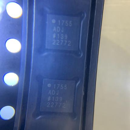
Image for reference only

Manufacturer Part:

ADP1755ACPZ-R7

Package:

LFCSP-16 EP (4 x 4 x 0.75 mm, 0.5mm pitch)

Brand:
Product Categories:
Other recommendations you may be interested in.
Description

The ADP1755ACPZ-R7 from Analog Devices is a 1.2 A low input voltage, adjustable output voltage, low dropout (LDO) linear regulator in a 16-lead LFCSP (4 mm x 4 mm with exposed pad) package with tape and reel packaging. Key specifications: input voltage range 1.6 V to 3.6 V; adjustable output voltage 0.75 V to 3.3 V via external resistor divider; reference voltage 0.5 V; maximum output current 1.2 A; dropout voltage 105 mV typical at 1.2 A load; initial output voltage accuracy plus or minus 1 percent; accuracy over line, load, and temperature plus or minus 2 percent; output noise 23 uV RMS at 0.75 V output; power supply rejection ratio (PSRR) 65 dB at 1 kHz, 65 dB at 10 kHz, 54 dB at 100 kHz; quiescent current 90 uA at IOUT = 500 uA, 400 uA at IOUT = 100 mA; shutdown current less than 2 uA; stable with 4.7 uF ceramic output capacitor; programmable soft start via external capacitor on SS pin; power-good (PG) output with open-drain; logic-controlled enable (EN) input; reverse current protection; current limit 1.5 A minimum; thermal overload protection; undervoltage lockout (UVLO); operating temperature -40 to +125 degrees C. The ADP1755 is the adjustable version; the ADP1754 is the fixed voltage version (7 options from 0.75 V to 2.5 V). RoHS compliant. Production status.

The ADP1755ACPZ-R7 from Analog Devices is a 1.2 A, low input voltage, adjustable output voltage, low dropout (LDO) linear regulator designed for powering noise-sensitive loads such as FPGAs, DSPs, microprocessors, and data converters from low-voltage input rails.

The ADP1755 is specifically optimized for low input/output voltage applications. The input voltage range of 1.6 V to 3.6 V means it is designed to regulate from common intermediate bus voltages such as 1.8 V, 2.5 V, and 3.3 V, and produce output voltages as low as 0.75 V. This makes it ideal for powering the core voltages of modern FPGAs and processors (0.9 V, 1.0 V, 1.1 V, 1.2 V) from a 1.8 V or 2.5 V rail.

The ADP1755 is the adjustable version of the ADP1754/ADP1755 family. The ADP1754 offers seven fixed output voltage options (0.75 V, 0.8 V, 0.9 V, 1.0 V, 1.2 V, 1.5 V, 2.5 V) for simplicity, while the ADP1755 allows any output voltage from 0.75 V to 3.3 V via an external resistor divider connected to the ADJ pin. The adjustable version is preferred when the output voltage is non-standard, when a single SKU must support multiple voltage rails, or when the output voltage must be fine-tuned.

The 0.5 V reference voltage at the ADJ pin means the output voltage is set by the formula VOUT = 0.5 V x (1 + R1/R2), where R1 is the upper resistor and R2 is the lower resistor. The low reference voltage enables output voltages close to 0.5 V, but the minimum guaranteed output voltage is 0.75 V due to the headroom required for the error amplifier and feedback network.

The 105 mV dropout voltage at 1.2 A is exceptionally low for a CMOS LDO, corresponding to an effective RDS(on) of approximately 88 mOhm. This allows the ADP1755 to regulate from a 1.8 V input down to a 1.5 V output at full 1.2 A load with only 105 mV of headroom. For a 1.2 V output at 1.2 A, the minimum input voltage is approximately 1.305 V, allowing regulation from a 1.5 V or 1.8 V rail.

The high PSRR of 65 dB at 1 kHz and 54 dB at 100 kHz makes the ADP1755 effective at rejecting switching power supply ripple and noise on the input rail. This is critical for FPGA and data converter applications where power supply noise directly impacts signal integrity and timing jitter. When the ADP1755 is used as a post-regulator after a switching converter, the combined PSRR can exceed 100 dB at 1 kHz, effectively eliminating switching ripple from the supply.

The 23 uV RMS output noise at 0.75 V output is very low for a 1.2 A LDO, ensuring that the regulated supply does not degrade the performance of noise-sensitive analog circuits such as ADCs and DACs. For even lower noise, an additional RC filter or ferrite bead can be added at the output, but in many applications the 23 uV RMS noise is sufficient without additional filtering.

The programmable soft start feature prevents inrush current during power-up. An external capacitor on the SS pin sets the startup ramp time; the soft start time is approximately 1 ms per 10 nF of capacitance. Without an external capacitor, the internal default soft start is active. Soft start is particularly important when the LDO is powering large FPGA core decoupling capacitor banks (10-100 uF) that would otherwise draw excessive inrush current.

The power-good (PG) output is an open-drain output that goes high-impedance when the output voltage is within the regulation window (typically above 90 percent of the set voltage). The PG output can be used to enable downstream loads, signal the system controller, or daisy-chain multiple LDO power-good signals for sequential power-up.

The reverse current protection feature prevents current from flowing backward from the output to the input when the input voltage drops below the output voltage. This is important in battery-powered applications where the battery may be removed while the output capacitor is still charged, or in systems with multiple power sources where one source may backfeed through the LDO.

At $1.26 per unit in volume (1000+), the ADP1755ACPZ-R7 is priced competitively for a 1.2 A, high-PSRR, low-noise LDO with power-good and soft-start features. It offers a more complete feature set than simpler LDOs (e.g., TPS73701) at a similar or lower price point.

The ADP1755ACPZ-R7 operates as a CMOS low dropout linear regulator using a P-channel MOSFET pass transistor controlled by a high-gain error amplifier.

Pass Transistor: The ADP1755 uses a P-channel MOSFET as the pass element between VIN and VOUT. The PMOS transistor is driven by the error amplifier output, which adjusts the gate voltage to maintain the desired output voltage. The PMOS pass transistor has a very low on-resistance (approximately 88 mOhm), which results in the 105 mV dropout voltage at 1.2 A. When the input-output voltage differential is less than the dropout voltage, the PMOS transistor operates in the linear (ohmic) region and acts as a variable resistor controlled by the error amplifier.

Error Amplifier and Feedback: The error amplifier compares a fraction of the output voltage (from the ADJ pin) with the internal 0.5 V reference. The output of the error amplifier drives the gate of the PMOS pass transistor to minimize the difference between the feedback voltage and the reference. The feedback divider consists of two external resistors (R1 and R2) connected between VOUT, ADJ, and GND. The output voltage is VOUT = 0.5 V x (1 + R1/R2). The error amplifier has high DC gain (typically 60-80 dB) to achieve excellent load and line regulation.

Reference Voltage: The internal 0.5 V bandgap reference is trimmed at the factory to achieve plus or minus 1 percent initial accuracy. The reference is designed to be stable over temperature, contributing to the overall plus or minus 2 percent accuracy over line, load, and temperature.

Dropout Operation: When the input voltage drops to within the dropout voltage of the output voltage (VIN less than VOUT + 105 mV at 1.2 A), the PMOS pass transistor enters the ohmic (triode) region. In this region, the regulator can no longer maintain the desired output voltage because the pass transistor is fully enhanced (minimum RDS(on)). The output voltage tracks the input voltage minus the IR drop across the pass transistor. The dropout voltage is proportional to the load current: VDO = IOUT x RDS(on) = IOUT x 88 mOhm.

Soft Start: The soft start circuit limits the inrush current during power-up by controlling the ramp rate of the output voltage. An external capacitor on the SS pin is charged by an internal current source, and the SS pin voltage controls the reference voltage ramp. The output voltage follows the SS pin voltage until it reaches the regulation set point. The soft start time is approximately tSS = CSS x VREF / ISS, where ISS is the internal charging current. With no external capacitor, the internal default ramp provides a fast but controlled startup.

Power-Good: The power-good comparator monitors the feedback voltage (ADJ pin) and compares it to a threshold (approximately 90 percent of the 0.5 V reference). When the feedback voltage is above the threshold, the PG output is high-impedance (open-drain off). When the feedback voltage drops below the threshold (indicating the output is out of regulation), the PG output pulls LOW through an internal N-channel MOSFET. The PG output requires an external pull-up resistor (typically 10-100 kOhm) to a logic supply.

PSRR: The high PSRR is achieved through the combination of the high-gain error amplifier, the PMOS pass transistor (which provides inherent supply rejection), and the internal compensation network. The PSRR decreases with frequency as the error amplifier gain rolls off, from 65 dB at 1 kHz to 54 dB at 100 kHz. At higher frequencies (above 100 kHz), the output capacitor provides additional filtering.

Current Limit: The current limit circuit monitors the current through the PMOS pass transistor using a scaled sense transistor. When the output current exceeds the current limit threshold (1.5 A minimum, typically 2.0 A), the error amplifier reduces the gate drive to the pass transistor, limiting the output current. The current limit is a foldback type that reduces the current limit under short-circuit conditions to reduce power dissipation.

Thermal Protection: A thermal sensor on the die monitors the junction temperature. When the junction temperature exceeds approximately 150 degrees C, the thermal shutdown circuit turns off the pass transistor. When the junction temperature drops below approximately 130 degrees C, the LDO restarts with the soft start sequence. The thermal shutdown has approximately 20 degrees C of hysteresis to prevent oscillation.

Reverse Current Protection: The reverse current protection circuit monitors the input and output voltages. When VOUT is higher than VIN (e.g., when the input supply is removed while the output capacitor is still charged), an internal circuit turns off the body diode of the PMOS pass transistor, preventing current from flowing from VOUT to VIN. This eliminates the need for an external Schottky diode across the LDO for reverse current protection.

Pin Name Type Description
1 VOUT Power Output Regulated output voltage; 0.75 V to 3.3 V adjustable; up to 1.2 A continuous; connect to load and output capacitor (4.7 uF ceramic minimum); the output capacitor must be placed within 5 mm of the pin; low-ESR X5R or X7R ceramic capacitor required; larger capacitance (up to 100 uF) improves load transient response and PSRR at high frequencies
2 VIN Power Input Unregulated input supply; 1.6 V to 3.6 V; must be at least VOUT + 105 mV at 1.2 A for regulation; connect to input capacitor (4.7 uF ceramic) placed close to the pin; the input capacitor must be rated for the maximum input voltage and have low ESR; connect VIN pins together externally
3 VIN Power Input Second VIN pin; must be connected to pin 2 externally; both VIN pins carry the input current and must be connected to the input supply with low-impedance traces
4 EN Input Enable input; active-high; CMOS and TTL compatible; pull HIGH (above 1.2 V) to enable the LDO; pull LOW (below 0.4 V) to disable the LDO and enter shutdown mode (less than 2 uA supply current); do not leave floating; connect to VIN through a 100 kOhm pull-up if always-on operation is desired; can be driven by a GPIO from a system controller for power sequencing
5 GND Ground Ground reference; connect to PCB ground plane; all GND pins must be connected together; the exposed pad on the bottom of the LFCSP package must be soldered to the ground plane for thermal dissipation; thermal resistance is approximately 33 degrees C/W (junction to ambient) with the exposed pad properly soldered
6 SS Input Soft start programming pin; connect an external capacitor (CSS) from SS to GND to set the startup ramp time; tSS (ms) = CSS (nF) x 0.1 (approximately); leave unconnected for default internal soft start (fast startup); the SS pin voltage ramps from 0 V to the reference voltage, controlling the output voltage ramp; during shutdown, the SS pin is discharged internally to reset the soft start
7 ADJ Input Output voltage adjustment feedback pin; connect to the midpoint of the external resistor divider between VOUT and GND; the internal reference voltage is 0.5 V; output voltage is VOUT = 0.5 V x (1 + R1/R2); use 1 percent or better resistors; R2 should be 10 kOhm or less to minimize feedback error; place the divider close to the ADJ pin; Kelvin-connect the top of R1 directly to VOUT at the load point for best regulation
8 PG Output Power-good open-drain output; goes high-impedance when output voltage is above the PG threshold (approximately 90 percent of set voltage); pulls LOW when output voltage is below threshold; requires an external pull-up resistor (10-100 kOhm) to a logic supply; can be used to enable downstream circuits or signal a system controller; remains LOW during shutdown, UVLO, current limit, and thermal shutdown
9-12 GND Ground Additional ground pins; connect to PCB ground plane; these pins provide the ground return for the internal circuitry and improve thermal dissipation; all GND pins and the exposed pad must be connected to the ground plane
13-14 VIN Power Input Additional VIN pins; connect to input supply; multiple VIN pins reduce parasitic inductance and distribute the input current; must be connected together externally
15-16 VOUT Power Output Additional VOUT pins; connect to output load and output capacitor; multiple VOUT pins reduce parasitic inductance and distribute the output current; must be connected together externally
EP Exposed Pad Ground/Thermal Exposed thermal pad on the bottom of the LFCSP package; must be soldered to the PCB ground plane with multiple thermal vias; this is the primary thermal dissipation path for the LDO; the thermal resistance from junction to ambient is approximately 33 degrees C/W with proper soldering; inadequate thermal connection will cause the junction temperature to rise excessively under heavy load
Application Description
FPGA Core Voltage Regulator Regulate 1.0 V core voltage for Xilinx or Intel FPGAs from a 1.8 V rail; 105 mV dropout allows headroom even at 1.2 A; 23 uV RMS noise does not degrade FPGA transceiver performance; PG output signals FPGA when core voltage is stable; soft start limits inrush current into large FPGA decoupling capacitor banks; 65 dB PSRR rejects switching supply ripple
Post-Regulator After DC-DC Place ADP1755 after a switching DC-DC converter to clean up the output; the DC-DC provides high efficiency step-down, and the ADP1755 provides low-noise, high-PSRR regulation; combined PSRR exceeds 100 dB at 1 kHz; ideal for noise-sensitive analog and RF circuits; the DC-DC output is set slightly above the desired voltage (e.g., 1.8 V in, 1.5 V out) to minimize LDO power dissipation
DSP/MCU Core Supply Provide low-noise core voltage for TI C6000 DSPs, ARM Cortex processors, or other high-performance digital ICs; adjustable output covers all common core voltages (0.9 V to 1.3 V); 1.2 A handles peak current demands; EN pin allows power sequencing with I/O voltage; PG output enables peripheral devices only after core is stable
ADC/DAC Voltage Reference Provide a clean, low-noise supply for high-resolution ADCs and DACs; 23 uV RMS noise contributes less than 0.5 LSB error at 12-bit, 2 V full-scale; 65 dB PSRR ensures switching supply noise does not couple into the analog supply; adjustable output can be set to the ADC/DAC reference voltage; use a pi-filter at the output for additional noise filtering if needed
Server Memory Power Regulate DDR4/DDR5 VDDQ (1.2 V) or VPP (2.5 V) from a 3.3 V or 2.5 V rail; 1.2 A handles multiple DIMM loads; fast transient response maintains regulation during memory read/write current transients; power-good monitors memory supply health; soft start prevents inrush during hot-swap events
Model Manufacturer Compatibility Key Difference
ADP1754ACPZ-R7 Analog Devices Same Family, Fixed Voltage Fixed voltage version of ADP1755; 7 options (0.75 V to 2.5 V); no external resistor divider needed; same LFCSP-16 package and pinout (ADJ pin is NC on fixed version); same electrical performance; use when a standard output voltage is needed and adjustability is not required; simpler BOM
TPS7A7001SLR TI Functional Equivalent 2 A LDO (higher current); 1.1-6.5 V input (wider range); 0.5-5.0 V adjustable output; 120 mV dropout at 2 A; higher PSRR (72 dB at 1 kHz); SOT-89-5 (smaller package but no PG output); no soft start; use when higher current or wider input range is needed and PG/SS are not required
NCP59302MNADTYG onsemi Functional Equivalent 3 A LDO (much higher current); 0.9-5.5 V input; 0.5-3.6 V adjustable output; DFN-8 (smaller package); higher dropout; lower PSRR; no soft start or PG in DFN package; use when higher current is the primary requirement and noise/PSRR are less critical
LT3021EDH Analog Devices Very Low Dropout 0.9-10 V input; 0.2-10 V adjustable; 500 mA (lower current); 160 mV dropout at 500 mA; very low input voltage capability (0.9 V); DFN-16; use when the input voltage is very low (below 1.6 V) and the ADP1755 cannot operate
ISL80102IRAJZ-TK Renesas Competitive Alternative 2 A LDO; 1.8-6 V input; 0.8-5 V adjustable; 130 mV dropout at 2 A; 70 dB PSRR at 1 kHz; DFN-8 (smaller package); no PG output; use as compact alternative with higher current but fewer features
Recommend Parts
Single-phase energy metering IC, <0.1% error, SPI, shunt/CT, LFCSP-28

Brand:

Package:

LFCSP-28 (5×5 mm)
In stock:
5098pcs

Cargo cycle: 3~7 Days
The minimum order is 1

Go to Inquiry
Dual high-speed op amp, 50MHz, 350V/µs, drives unlimited Cload, 8-SOIC

Brand:

Package:

8-SOIC (3.9×5.0×1.5 mm)
In stock:
7183pcs

Cargo cycle: 3~7 Days
The minimum order is 1

Go to Inquiry
1024-position nonvolatile digital potentiometer, 10kΩ, SPI, EEMEM, 16-TSSOP, REEL7 packaging

Brand:

Package:

16-TSSOP (5.0×4.4mm)
In stock:
9739pcs

Cargo cycle: 3~7 Days
The minimum order is 1

Go to Inquiry
Transformer-coupled isolation amplifier, 750Vrms isolation, 2kHz bandwidth, 10-DIP, with integrated isolated power

Brand:

Package:

10-Pin DIP
In stock:
14100pcs

Cargo cycle: 3~7 Days
The minimum order is 1

Go to Inquiry
8-ch 12-bit 454kSPS ADC DAS, bipolar inputs, parallel/serial, 44-MQFP, 5V supply

Brand:

Package:

MQFP-44 (10 x 10 mm)
In stock:
9131pcs

Cargo cycle: 3~7 Days
The minimum order is 1

Go to Inquiry
Quad 8-bit voltage output DAC, 4-channel, MPU-compatible, 20-SOIC, no external trims

Brand:

Package:

SOIC-20 (Wide) (7.5 x 12.8 mm)
In stock:
5393pcs

Cargo cycle: 3~7 Days
The minimum order is 1

Go to Inquiry
Quality Assurance

All electronic components we source from our partnered supply chains go through strict incoming inspections.Through careful testing, we ensure everything delivered to customers is genuine original parts and meets quality requirements.In addition, we keep complete inspection records to make the entire supply chain process clear and traceable.

Certification
We have obtained a number of professional certifications and built our own professional testing laboratory.This ensures that every product we deliver to our customers meets the highest quality requirements.We conduct tests in strict accordance with procedures to ensure stable product quality and accurate parameters.To guarantee genuine original parts, we also cooperate with reliable third-party testing institutions for strict quality inspection.We always attach great importance to quality and fully comply with industry standards, relevant regulations, and ISO 9001:2015 requirements.

Shipping & Payment

All electronic components we source from our partnered supply chains go through strict incoming inspections.Through careful testing, we ensure everything delivered to customers is genuine original parts and meets quality requirements.In addition, we keep complete inspection records to make the entire supply chain process clear and traceable.

Certification
We have obtained a number of professional certifications and built our own professional testing laboratory.This ensures that every product we deliver to our customers meets the highest quality requirements.We conduct tests in strict accordance with procedures to ensure stable product quality and accurate parameters.To guarantee genuine original parts, we also cooperate with reliable third-party testing institutions for strict quality inspection.We always attach great importance to quality and fully comply with industry standards, relevant regulations, and ISO 9001:2015 requirements.

Service & Packaging

All electronic components we source from our partnered supply chains go through strict incoming inspections.Through careful testing, we ensure everything delivered to customers is genuine original parts and meets quality requirements.In addition, we keep complete inspection records to make the entire supply chain process clear and traceable.

Certification
We have obtained a number of professional certifications and built our own professional testing laboratory.This ensures that every product we deliver to our customers meets the highest quality requirements.We conduct tests in strict accordance with procedures to ensure stable product quality and accurate parameters.To guarantee genuine original parts, we also cooperate with reliable third-party testing institutions for strict quality inspection.We always attach great importance to quality and fully comply with industry standards, relevant regulations, and ISO 9001:2015 requirements.



