
The semiconductor industry is currently facing a prominent structural contradiction. With the rapid advancement of intelligent driving, computing power demands have risen exponentially, soaring from dozens of TOPS for L2+ assisted driving to thousands of TOPS required for L4/L5 high-level autonomous driving. Meanwhile, Moore’s Law is approaching its physical limits, creating growing research and mass-production bottlenecks for advanced-process monolithic SoCs.
Monolithic SoCs integrating tens of billions of transistors on 2nm and 3nm processes require mask costs reaching tens of millions of US dollars, while chip yield declines exponentially with increasing integration density. Compared with consumer-grade chips, automotive chips impose far stricter industrial standards: they must deliver extreme AI computing performance while satisfying high reliability, wide-temperature resistance, and a 15-year extended service life requirement. In this context, Chiplet technology, initially adopted in data centers, has achieved large-scale deployment in automotive applications.
Breaking the traditional monolithic SoC design philosophy of integrating all functions on a single silicon die, the Chiplet architecture disassembles a complete chip system into multiple functionally dedicated bare dies and reintegrates them via advanced packaging technologies. This represents not only an upgrade in semiconductor manufacturing processes but also a disruptive transformation in chip architecture design, driving the industry’s evolution from function-defined architecture to connection-defined architecture.

I. Heterogeneous Chiplet SoC Architecture: An Optimal Customizable Solution
Traditional monolithic SoCs suffer from inherent design limitations, as all functional modules must share the same manufacturing process, making it impossible to balance performance, cost, and reliability. The core design philosophy of the Chiplet architecture is customization on demand and optimal ratio configuration. Its asymmetric process layout enables extreme adaptation for each functional module, perfectly matching the differentiated requirements of automotive central computing platforms.
1. Differentiated Process Deployment for Functional Chiplets
Compute Die: Adopts cutting-edge 3nm process technology, integrating automotive-optimized Arm Neoverse V3AE high-performance CPU clusters and NPU cores dedicated to large-model inference. As demonstrated by flagship automotive computing platforms such as NVIDIA Thor, advanced processes effectively suppress power overflow under full AI load and ensure stable high-performance computing for advanced intelligent driving.
I/O & Safety Die: Adopts mature and automotive-qualified 12nm/22nm processes, integrating analog circuits, power management modules, and ASIL-D compliant lock-step safety MCUs. For these modules, advanced processes deliver negligible area reduction while causing severe leakage current issues. Adopting mature processes significantly cuts R&D and manufacturing costs while leveraging superior process stability to meet the high-reliability and long-lifecycle requirements of automotive-grade chips.
2. Innovation in Storage Architecture: Breaking the Intelligent Driving Storage Wall
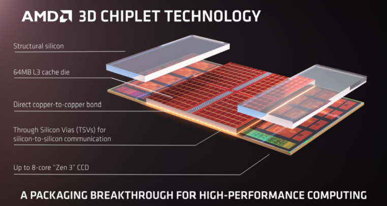
The core bottleneck of intelligent driving computing lies not in logical arithmetic capability, but in the high-speed transmission and reading/writing of massive perception data. In 2026, mainstream automotive chips adopt LPDDR5X/5T memory with a maximum data rate of 9.6Gbps, which still fails to meet the high-frequency data interaction demands of high-level intelligent driving.
The Chiplet architecture adopts a near-memory computing design, physically aligning memory controllers with computing cores to shorten data transmission paths and reduce latency significantly. Meanwhile, the industry widely adopts AMD V-Cache style 3D-stacked SRAM technology, deploying high-capacity L3/L4 cache chiplets to minimize data exchange latency across dies. This provides a solid hardware foundation for high-frequency read-write AI algorithms such as timing anomaly detection and real-time environmental perception.
II. High-Speed Interconnection System: The Core Foundation of Chiplet Architecture
If functional chiplets serve as the core components of automotive SoCs, high-speed interconnection acts as the neural system that links all modules to achieve collaborative operation, directly determining the overall performance ceiling and system stability.
1. UCIe 2.0/3.0: The Universal Standard for Automotive Chiplet Interconnection
After years of industrial protocol iteration, UCIe (Universal Chiplet Interconnect Express) has become the de facto standard for automotive-grade Chiplet chips. Featuring decoupled physical and protocol layers, the UCIe architecture supports CXL and PCIe compatibility, delivering excellent ecological universality.
Mass-production automotive chips in 2026 are predominantly equipped with UCIe 2.0, while high-end flagship platforms have deployed UCIe 3.0 with optimized physical-layer anti-interference performance and robustness. Tailored for automotive extreme temperature conditions ranging from -40℃ to 125℃, UCIe integrates a runtime recalibration mechanism that dynamically adjusts signal drive strength and equalizer parameters according to ambient temperature. It maintains an extremely low bit error rate even at a ultra-high transmission rate of 64GT/s, fully adapting to complex automotive operating conditions.
2. Tiered Packaging Solutions: Balancing Performance and Cost
Packaging technology determines the ultimate performance of cross-chiplet interconnection. Currently, two mature tiered packaging solutions have been formed for automotive scenarios to meet the demands of different vehicle grades:
Passive Silicon Interposer (CoWoS-S): The most mature high-end packaging solution in the industry, achieving stable multi-chiplet interconnection through high-density wiring on silicon substrates with high bandwidth and outstanding stability, suitable for flagship high-level intelligent driving platforms.
Embedded Silicon Bridge (Si-Bridge): Inspired by Intel EMIB technology, this solution embeds miniature silicon slices only at chiplet docking positions. It retains high-bandwidth transmission capability while substantially reducing packaging costs, making it the mainstream cost-effective solution for mid-to-high-end vehicles in 2026.
III. Core Engineering Challenges of Automotive Chiplet Architecture
While the Chiplet architecture effectively resolves the computing power, cost, and process bottlenecks of traditional monolithic SoCs, it still faces multiple rigorous engineering challenges in latency, heat dissipation, power supply, and testing certification under strict automotive-grade standards.
1. Deterministic Latency Challenges Restricting Real-Time Computing Deployment
Cross-chiplet communication is not completely lossless. Engineering tests show that cross-die data access latency ranges from 5ns to 12ns, 2–3 times that of L3 cache latency in monolithic SoCs, accompanied by random jitter. For ultra-real-time autonomous driving algorithms such as planning and control, minor latency fluctuations may induce potential system risks.
Furthermore, heterogeneous multi-chiplet architectures rely on NoC (Network-on-Chip) to build a unified global memory address space. Managing cache consistency among heterogeneous CPU, GPU, and NPU cores and avoiding data deadlock and memory collapse constitute core architectural design challenges.
2. Power Supply and Thermodynamic Constraints Limiting Hardware Stability
Automotive computing chips feature ultra-compact size. Within a silicon area of less than 100 square millimeters, transient current dynamically switches between 30A and 60A, imposing extreme pressure on the power distribution network (PDN). Chiplets are interconnected via micro-bumps with limited current-carrying capacity, easily triggering IR-Drop voltage drop under full computing load, which may cause logical operation errors and system reboot failures.
In addition, heterogeneous chiplets suffer from uneven heat distribution: NPU cores generate high-temperature hotspots under heavy load, while adjacent I/O and safety die remain relatively cool. Thermal gradient-induced CTE (Coefficient of Thermal Expansion) mismatch generates continuous mechanical stress, which may fracture interconnection points during long-term operation. Precise thermal simulation modeling and dynamic thermal management scheduling algorithms are required for optimization.
3. KGD Quality Control Increases Supply Chain and Testing Difficulties
In traditional monolithic chip design, a single failed chip can be scrapped independently. In contrast, Chiplet packaging is an integrated structure: if any bare die fails after packaging, the entire high-cost packaged chip must be discarded, significantly increasing mass production losses.
Moreover, conventional ATE (Automatic Test Equipment) cannot detect internal interconnection links of multi-chiplet packages, making full hidden hazard inspection extremely difficult. The complexity of automotive-grade reliability testing has driven the deployment of new technologies such as AI-based real-time chip health prediction and link anomaly monitoring.
IV. SDV Software Definition: Shielding Hardware Complexity and Enabling Unified Computing Scheduling
To adapt to heterogeneous Chiplet architectures and lower upper-layer development thresholds, the SDV (Software-Defined Vehicle) system provides comprehensive supporting capabilities to transparently shield underlying hardware complexity.
On one hand, the Hypervisor virtualization layer abstracts the underlying Chiplet physical topology, shielding multi-die and multi-process hardware differences. Upper-layer autonomous driving applications access a unified computing resource pool without perceiving underlying hardware segmentation.
On the other hand, dedicated heterogeneous computing compilers intelligently split large-model operators and dynamically assign tasks to different chiplets based on computing power and bandwidth resources. The strategy of “parallel computing and data transmission” offsets additional latency caused by cross-chiplet interconnection and maximizes the computing potential of heterogeneous architectures.
V. Conclusion: Chiplet as the Inevitable Path for Automotive Central Computing
Modern automotive chip design has moved beyond the extensive model of simply stacking TOPS computing power. The Chiplet architecture delivers an innovative engineering logic: architecture follows connection, and function adapts to scenarios.
Through modular heterogeneous integration, Chiplet adopts advanced processes to meet the extreme computing demands of high-level intelligent driving, while leveraging mature processes to guarantee automotive functional safety and long-term reliability. Its flexible architecture adapts to iterating AI algorithms, perfectly balancing four core indicators: performance, cost, reliability, and service life.
In the wave of integrated automotive central computing evolution, Chiplet is not an optional technology, but an inevitable industrial upgrade path. Every optimization in latency, energy efficiency, and stability represents rigorous engineering practice that drives automotive semiconductor technology from theoretical research to large-scale industrial maturity.
 English
  简体中文
简体中文  Español
  العربية