TLV62569PDDCT


2A synchronous buck converter, 2.5-5.5V input, 0.6-5.5V output, 1.5MHz, PSM, TSOT-23-6 thin

4818

Effective Inventory
Go to Inquiry

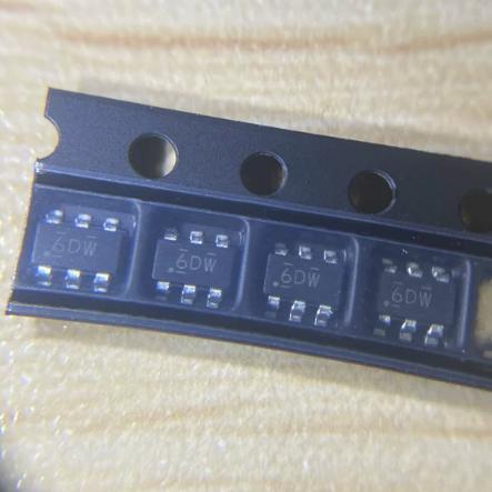
Image for reference only

Manufacturer Part:

TLV62569PDDCT

Package:

TSOT-23-6 Thin (3.05 x 1.75 mm)

Brand:
Product Categories:
Other recommendations you may be interested in.
Description

The TLV62569PDDCT is a 2A synchronous step-down buck DC-DC converter from Texas Instruments in a TSOT-23-6 Thin (3.05 x 1.75 mm) package. It operates from 2.5V to 5.5V input with adjustable output from 0.6V to 5.5V, switching at 1.5 MHz in PWM mode with automatic Power Save Mode (PSM) at light loads for high efficiency across the entire load range. Features include internal soft-start, overcurrent protection with hiccup mode, thermal shutdown, power-good output, and less than 2 µA shutdown current. Achieves up to 95% efficiency. The PDDCT variant ships in small tape and reel (250/reel); the PDDCR variant ships in large tape and reel (3,000/reel). Operating temperature: -40°C to +125°C (TJ). MSL-1, RoHS3 compliant.

The TLV62569PDDCT is a 2-A high-efficiency synchronous step-down (buck) DC-DC converter manufactured by Texas Instruments, optimized for compact solution size and high efficiency across a wide load current range. It integrates both high-side and low-side MOSFET switches, requiring only an inductor, input/output capacitors, and a feedback resistor divider to form a complete power supply.

The device operates from an input voltage range of 2.5V to 5.5V, making it ideal for single-cell Li-Ion battery-powered applications, 3.3V and 5V rail point-of-load conversions, and USB-powered devices. The output voltage is adjustable from 0.6V to 5.5V via an external resistor divider, with the 0.6V reference voltage enabling very low output voltages for modern low-voltage processors and FPGAs.

At medium to heavy loads, the TLV62569 operates in pulse width modulation (PWM) mode with a fixed 1.5 MHz switching frequency, enabling the use of small external inductors (typically 1.0-2.2 µH) and ceramic capacitors for a compact solution footprint. At light loads, the device automatically enters Power Save Mode (PSM), skipping pulses to maintain high efficiency by reducing switching losses. In PSM, the device operates in hysteretic mode with reduced switching frequency, minimizing quiescent current draw.

The TLV62569 features an internal soft-start circuit that limits inrush current during startup, overcurrent protection (OCP) with hiccup mode for fault recovery, thermal shutdown protection, and a power-good indicator. The shutdown current is less than 2 µA, making it suitable for always-on battery-powered systems where standby power consumption must be minimized.

The PDDCT package is a TSOT-23-6 Thin (6-pin Thin Small Outline Transistor) measuring 3.05 x 1.75 mm maximum, among the smallest footprints available for a 2A buck converter. The T suffix denotes small tape and reel packaging (250/reel), while the R suffix (PDDCR) denotes large tape and reel (3,000/reel). Both are electrically identical. The device achieves up to 95% efficiency and operates over a junction temperature range of -40°C to +125°C.

The TLV62569PDDCT operates as a current-mode synchronous buck (step-down) DC-DC converter, converting a higher input voltage to a lower regulated output voltage with high efficiency through high-frequency switching and synchronous rectification.

Synchronous Buck Topology: The converter integrates two N-channel MOSFET switches: a high-side switch (connected between VIN and the SW node) and a low-side switch (connected between the SW node and GND). During the ON-time, the high-side switch closes and current flows from VIN through the inductor to the output capacitor and load, storing energy in the inductor magnetic field. During the OFF-time, the high-side switch opens and the low-side switch closes, providing a path for the inductor current to freewheel through the low-side switch to GND. The synchronous rectifier (low-side MOSFET) replaces the traditional Schottky diode, significantly reducing conduction losses and improving efficiency, especially at low output voltages where diode forward voltage represents a large fraction of the output.

Current-Mode Control: The device uses peak current-mode control, where the error amplifier output (proportional to the difference between the feedback voltage and the 0.6V internal reference) sets the peak inductor current threshold for each switching cycle. The high-side switch turns on at the beginning of each cycle, and the inductor current ramps up linearly. When the sensed current reaches the threshold set by the error amplifier, the high-side switch turns off and the low-side switch turns on. This control method provides inherent cycle-by-cycle current limiting, fast transient response, and easy loop compensation.

PWM Mode: At load currents above the PSM threshold (typically around 100 mA), the device operates in continuous conduction mode (CCM) with fixed 1.5 MHz switching frequency. The duty cycle is approximately D = VOUT / VIN under ideal conditions. The fixed frequency operation ensures predictable EMI performance and enables the use of small, low-profile inductors and ceramic capacitors.

Power Save Mode (PSM): When the load current drops below the PSM threshold, the device transitions to pulse frequency modulation (PFM) mode. In PSM, the high-side switch is pulsed only when the output voltage drops below a threshold slightly below the regulation target, and multiple pulses may be skipped between active pulses. This dramatically reduces switching losses at light loads because the MOSFETs switch much less frequently. The switching frequency in PSM varies proportionally with load current, from a few kHz at very light loads up to the 1.5 MHz PWM frequency at the PSM-to-PWM transition point. This keeps quiescent current very low at standby.

Voltage Feedback: The output voltage is sensed through an external resistor divider connected between VOUT, the FB (feedback) pin, and GND. The FB pin is compared against the 0.6V internal reference by the error amplifier. The output voltage is set by: VOUT = 0.6V × (1 + R1/R2), where R1 is the upper resistor and R2 is the lower resistor. Choosing appropriate resistor values (typically in the 100 kΩ-1 MΩ range) sets the desired output voltage while minimizing divider current.

Soft Start: At power-up or when exiting shutdown, the internal soft-start circuit gradually increases the current limit threshold over approximately 1 ms, allowing the output voltage to ramp up smoothly without overshoot or excessive inrush current that could trigger OCP.

Protection: Overcurrent protection (OCP) limits the peak inductor current on a cycle-by-cycle basis. If an overcurrent condition persists, the device enters hiccup mode, periodically retrying to recover from the fault. Thermal shutdown disables the device when the junction temperature exceeds approximately 150°C, with automatic recovery after the device cools below the hysteresis threshold.

Pin Name Type Default Function Description
1 GND G Ground Power and signal ground; connect to PCB ground plane and thermal pad
2 SW O Switch Node Output of the internal high-side/low-side MOSFET half-bridge; connect to inductor
3 VIN I Input Supply Power input, 2.5V to 5.5V; requires ceramic bypass capacitor to GND close to pin
4 EN I Enable Active-high enable input; pull HIGH (>1.2V) to enable; pull LOW (<0.4V) to enter shutdown (<2 µA IQ); do not float
5 FB I Feedback Output voltage feedback input; connect to external resistor divider from VOUT to GND; reference voltage 0.6V
6 PG O Power Good Active-high power-good indicator; HIGH when output is in regulation; can be left unconnected if not used
Application Description
Battery-Powered Devices Point-of-load regulation from single-cell Li-Ion (2.7-4.2V) to 1.2V/1.8V/3.3V rails in smartphones, tablets, and portable instruments; PSM maximizes battery life at light loads
5V/3.3V Rail Point-of-Load Step-down from 5V or 3.3V system rails to lower voltages (1.0V, 1.2V, 1.8V, 2.5V) for processors, FPGAs, and peripherals; ultra-small TSOT-23-6 footprint saves board space
USB-Powered Devices Regulating 5V USB bus voltage to 3.3V or lower for USB peripherals, hubs, and adapters; wide input range tolerates USB voltage variations
IoT and Wearables Compact, high-efficiency power conversion for IoT sensor nodes and wearable devices where board area and battery life are critical; <2 µA shutdown current
Embedded Computing Core and I/O voltage regulation for ARM SoCs, microcontrollers, and wireless modules in embedded systems; 2A output supports moderate compute loads
Model Manufacturer Compatibility Key Difference
TLV62569PDDCR TI Pin-Compatible / Electrically Identical Large tape and reel packaging (3,000/reel) vs small reel (250/reel); preferred for volume production
TLV62568PDDCR TI Pin-Compatible 1A output current version; same package, pinout, and switching frequency; lower current rating for lighter loads
TLV62569PDRL TI Functionally Identical SOT-563-6 (DRl) package variant; even smaller footprint (1.6 x 1.6 mm); same electrical specs
TPS562201DDCR TI Functionally Similar 2A buck, 4.5-17V input, 580 kHz, D-CAP2 control; wider input range but lower frequency; different control method
SY8089AAC Silergy Functionally Similar 2A buck, 2.5-5.5V input, 1.5 MHz, SOT-23-5; comparable specs but 5-pin package without PG output
Recommend Parts
PMIC for AM335x, 3 bucks, 2 LDOs, battery charger, WLED, I2C, VQFN-48

Brand:

Package:

VQFN-48 (6×6 mm, 0.4 mm pitch)
In stock:
8909pcs

Cargo cycle: 3~7 Days
The minimum order is 1

Go to Inquiry
Octal D-type flip-flop, edge-triggered, async clear, 28MHz, SOP-20

Brand:

Package:

SOP-20 (NS) (12.6×7.8 mm)
In stock:
8359pcs

Cargo cycle: 3~7 Days
The minimum order is 1

Go to Inquiry
3-to-8 decoder/demux, active-low outputs, 3 enable inputs, 15ns, PDIP-16

Brand:

Package:

PDIP-16 (24.33×9.4 mm, Through-Hole)
In stock:
11952pcs

Cargo cycle: 3~7 Days
The minimum order is 1

Go to Inquiry
2W mono Class-AB audio amp, BTL speaker + SE headphone, 2.5-5.5V, HVSSOP-8

Brand:

Package:

HVSSOP-8 (DGN) (3.0×4.9 mm, PowerPAD)
In stock:
3337pcs

Cargo cycle: 3~7 Days
The minimum order is 1

Go to Inquiry
10/100 Ethernet PHY, MII/RMII/SNI, Auto-MDIX, 270mW, LQFP-48, commercial

Brand:

Package:

LQFP-48 (7×7 mm)
In stock:
14754pcs

Cargo cycle: 3~7 Days
The minimum order is 1

Go to Inquiry
Octal bus transceiver, 3-state outputs, 2-6V, 12ns tpd, TSSOP-20

Brand:

Package:

TSSOP-20 (6.5×6.4 mm)
In stock:
2638pcs

Cargo cycle: 3~7 Days
The minimum order is 1

Go to Inquiry
Quality Assurance

All electronic components we source from our partnered supply chains go through strict incoming inspections.Through careful testing, we ensure everything delivered to customers is genuine original parts and meets quality requirements.In addition, we keep complete inspection records to make the entire supply chain process clear and traceable.

Certification
We have obtained a number of professional certifications and built our own professional testing laboratory.This ensures that every product we deliver to our customers meets the highest quality requirements.We conduct tests in strict accordance with procedures to ensure stable product quality and accurate parameters.To guarantee genuine original parts, we also cooperate with reliable third-party testing institutions for strict quality inspection.We always attach great importance to quality and fully comply with industry standards, relevant regulations, and ISO 9001:2015 requirements.

Shipping & Payment

All electronic components we source from our partnered supply chains go through strict incoming inspections.Through careful testing, we ensure everything delivered to customers is genuine original parts and meets quality requirements.In addition, we keep complete inspection records to make the entire supply chain process clear and traceable.

Certification
We have obtained a number of professional certifications and built our own professional testing laboratory.This ensures that every product we deliver to our customers meets the highest quality requirements.We conduct tests in strict accordance with procedures to ensure stable product quality and accurate parameters.To guarantee genuine original parts, we also cooperate with reliable third-party testing institutions for strict quality inspection.We always attach great importance to quality and fully comply with industry standards, relevant regulations, and ISO 9001:2015 requirements.

Service & Packaging

All electronic components we source from our partnered supply chains go through strict incoming inspections.Through careful testing, we ensure everything delivered to customers is genuine original parts and meets quality requirements.In addition, we keep complete inspection records to make the entire supply chain process clear and traceable.

Certification
We have obtained a number of professional certifications and built our own professional testing laboratory.This ensures that every product we deliver to our customers meets the highest quality requirements.We conduct tests in strict accordance with procedures to ensure stable product quality and accurate parameters.To guarantee genuine original parts, we also cooperate with reliable third-party testing institutions for strict quality inspection.We always attach great importance to quality and fully comply with industry standards, relevant regulations, and ISO 9001:2015 requirements.



