The SN74LVC1G08DCKR from Texas Instruments is a single 2-input positive-AND gate housed in an ultra-compact SC-70-5 (SOT-353) package, performing the Boolean function Y = A AND B (or Y = NOT(A OR B) in DeMorgan equivalent form) in positive logic.
The device is part of the 74LVC (Low-Voltage CMOS) family, designed to operate over a wide VCC range of 1.65V to 5.5V. This makes it suitable for 1.8V, 2.5V, 3.3V, and 5V logic systems. The inputs accept voltages up to 5.5V regardless of VCC, enabling the device to serve as a voltage translator: a 5V input signal can drive the AND gate while the output swings to the VCC level (e.g., 3.3V), providing down-translation without level shifter ICs.
Key performance specifications include: maximum propagation delay of 3.6ns at 3.3V (4ns at 5V) with 50pF load, output drive current of plus/minus 24mA at 3.3V and plus/minus 32mA at 5V in push-pull CMOS configuration, and maximum quiescent current of 10uA. The push-pull output provides strong drive with rail-to-rail swing, unlike open-drain alternatives that require external pullup resistors.
The Ioff feature is critical for mixed-voltage and hot-swap applications: when VCC is at 0V (device powered down), the Ioff circuitry disables the output, preventing damaging current from flowing back through the device from the input or output pins. This allows the device to be used in systems where different voltage domains may be powered independently, and supports live insertion (hot-swap) of cards or modules.
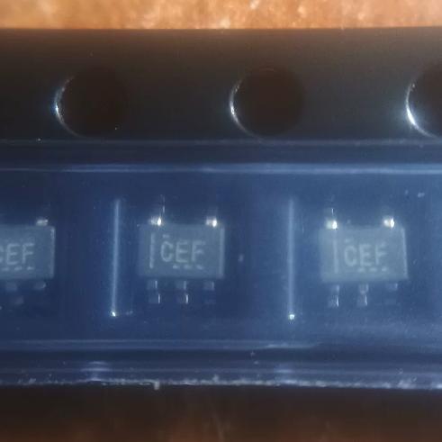
The DCK suffix denotes the SC-70-5 package, while the R suffix denotes tape and reel packaging with 3,000 units per reel. The device is also available in SOT-23-5 (DBV), SOT-5X3 (DRL), DSBGA-5 (YZP), USON-6 (DRY), X2SON-5 (DPW, ultra-small 0.8×0.8mm), and X2SON-6 (DSF) packages. The device is RoHS compliant, MSL Level 1, and classified as EAR99. Operating temperature range is -40C to 125C (TA), suitable for industrial and automotive-adjacent applications.





 English
  简体中文
简体中文  Español
  العربية