SN74LVC1G08DCKR


Single 2-input AND gate, 1.65-5.5V, 5V-tolerant inputs, 3.6ns tpd, Ioff, SC-70-5, -40~125C

166264

المخزون الفعال

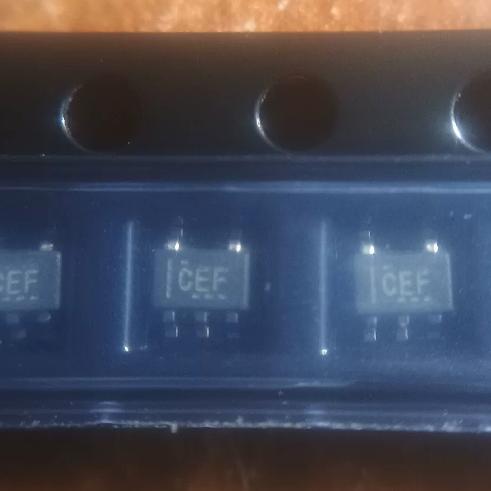
Image for reference only

جزء الشركة المصنعة : جزء الشركة المصنعة

SN74LVC1G08DCKR

الحزمة : الحزمة

SC-70-5 / SOT-353 (2.0 x 2.1 x 1.0 mm)

العلامة التجارية : العلامة التجارية
توصيات أخرى قد تكون مهتماً بها.
الوصف

The SN74LVC1G08DCKR from Texas Instruments is a single 2-input positive-AND gate in an SC-70-5 (SOT-353) package, performing the Boolean function Y = A AND B. The device operates from 1.65V to 5.5V VCC with 5.5V-tolerant inputs, making it suitable for both 3.3V and 5V systems as well as voltage translation between them. Maximum propagation delay: 3.6ns at 3.3V, 4ns at 5V. Output drive: plus/minus 24mA at 3.3V, plus/minus 32mA at 5V (push-pull CMOS output). Quiescent current: 10uA max. The Ioff feature supports partial-power-down mode operation by disabling the outputs when VCC = 0V, preventing damaging backflow current. Latch-up exceeds 100mA per JESD 78 Class II. ESD protection exceeds 2000V HBM, 200V MM, 1000V CDM. Operating temperature: -40C to 125C. Package dimensions: 2.0 x 2.1 x 1.0 mm. Tape and reel, 3000/reel. RoHS, EAR99.

The SN74LVC1G08DCKR from Texas Instruments is a single 2-input positive-AND gate housed in an ultra-compact SC-70-5 (SOT-353) package, performing the Boolean function Y = A AND B (or Y = NOT(A OR B) in DeMorgan equivalent form) in positive logic.

The device is part of the 74LVC (Low-Voltage CMOS) family, designed to operate over a wide VCC range of 1.65V to 5.5V. This makes it suitable for 1.8V, 2.5V, 3.3V, and 5V logic systems. The inputs accept voltages up to 5.5V regardless of VCC, enabling the device to serve as a voltage translator: a 5V input signal can drive the AND gate while the output swings to the VCC level (e.g., 3.3V), providing down-translation without level shifter ICs.

Key performance specifications include: maximum propagation delay of 3.6ns at 3.3V (4ns at 5V) with 50pF load, output drive current of plus/minus 24mA at 3.3V and plus/minus 32mA at 5V in push-pull CMOS configuration, and maximum quiescent current of 10uA. The push-pull output provides strong drive with rail-to-rail swing, unlike open-drain alternatives that require external pullup resistors.

The Ioff feature is critical for mixed-voltage and hot-swap applications: when VCC is at 0V (device powered down), the Ioff circuitry disables the output, preventing damaging current from flowing back through the device from the input or output pins. This allows the device to be used in systems where different voltage domains may be powered independently, and supports live insertion (hot-swap) of cards or modules.

The DCK suffix denotes the SC-70-5 package, while the R suffix denotes tape and reel packaging with 3,000 units per reel. The device is also available in SOT-23-5 (DBV), SOT-5X3 (DRL), DSBGA-5 (YZP), USON-6 (DRY), X2SON-5 (DPW, ultra-small 0.8×0.8mm), and X2SON-6 (DSF) packages. The device is RoHS compliant, MSL Level 1, and classified as EAR99. Operating temperature range is -40C to 125C (TA), suitable for industrial and automotive-adjacent applications.

The SN74LVC1G08DCKR implements a 2-input AND logic function using CMOS transistor-level circuitry in a single-gate configuration.

CMOS AND Gate Implementation: A CMOS AND gate is typically implemented by combining a NAND gate with an inverter. The NAND gate uses complementary PMOS and NMOS transistor networks: the PMOS network connects VCC to the output when either input is LOW (parallel PMOS configuration), while the NMOS network connects the output to GND only when both inputs are HIGH (series NMOS configuration). The subsequent inverter stage complements the NAND output to produce the AND function: Y = A AND B.

Voltage Translation: The 5.5V-tolerant input capability works because the input protection and level-shifting circuitry can accept voltages higher than VCC without forward-biasing internal parasitic diodes. When a 5V signal is applied to an input while VCC = 3.3V, the internal circuitry correctly recognizes the logic level and drives the output to VCC (3.3V). This provides unidirectional down-translation from 5V to 3.3V logic. Note that up-translation (VCC = 5V with 3.3V inputs) is also supported since the 3.3V HIGH level exceeds the VIH threshold at 5V VCC.

Ioff Partial Power-Down: The Ioff circuitry consists of isolation transistors that disconnect the output stage when VCC drops below a threshold. When VCC = 0V, the Ioff circuitry ensures that the output enters a high-impedance state, preventing current from flowing from the input pins (which may still be at logic HIGH from another active domain) through internal ESD diodes or parasitic paths to the VCC rail. This is essential for: (1) mixed-voltage systems where some domains are powered while others are not, (2) hot-swap applications where cards are inserted/removed while power is applied, and (3) battery backup systems where the main logic is powered down but interface signals remain active.

Output Drive: The push-pull CMOS output stage uses complementary PMOS (pull-up) and NMOS (pull-down) transistors. The PMOS transistor sources current when driving the output HIGH (up to VOH specification), and the NMOS transistor sinks current when driving the output LOW (up to VOL specification). The plus/minus 24mA drive at 3.3V provides sufficient current to drive multiple logic inputs, short PCB traces, and moderate capacitive loads without additional buffering.

Propagation Delay: The 3.6ns maximum propagation delay at 3.3V (50pF load) includes both the NAND and inverter stages. The delay is relatively insensitive to VCC within the operating range due to the CMOS design. At 5V VCC, the increased gate overdrive reduces propagation delay to 4ns maximum while increasing output drive to plus/minus 32mA.

دبوس الاسم النوع الوصف
1 A المدخلات AND gate input A; 5.5V-tolerant; CMOS input with very low input current (0.1uA typical); VIH and VIL thresholds scale with VCC
2 B المدخلات AND gate input B; 5.5V-tolerant; CMOS input; Y = A AND B in positive logic; both inputs must be HIGH for HIGH output
3 GND الطاقة Ground; connect to system ground plane; serves as reference for all input and output logic levels
4 Y المخرجات AND gate output; push-pull CMOS; HIGH when both A and B are HIGH; LOW otherwise; drives up to plus/minus 24mA at 3.3V; high-impedance when VCC = 0V (Ioff)
5 VCC الطاقة Supply voltage; 1.65V to 5.5V; bypass with 0.1uF ceramic capacitor to GND; determines output voltage levels and propagation delay
التطبيق الوصف
Enable Gating Generate gated enable signals where an enable input ANDed with a clock or data signal produces a controlled output; Y = Enable AND Clock; useful for conditional clock distribution
Voltage Level Translation 5V-tolerant inputs enable down-translation from 5V to 3.3V logic; AND gate combines level-shifting with logic function in a single gate; eliminates dedicated level-shifter ICs for single signals
Condition Monitoring AND two status signals to detect when both conditions are met simultaneously; Y = StatusA AND StatusB; used in safety interlocks, power-good detection, and fault monitoring
Hot-Swap/Hot-Plug Systems Ioff feature prevents back-drive current when VCC is removed; AND gate in card edge circuitry stays high-impedance during card insertion/removal; supports live insertion without bus contention
Board Space Optimization SC-70-5 package (2.0 x 2.1 mm) replaces a full quad AND gate IC when only one gate is needed; saves board space, reduces cost, and simplifies routing in dense designs
الطراز الشركة المصنعة التوافق الفرق الرئيسي
SN74LVC1G08DBVR TI متطابق وظيفيًا SOT-23-5 package (2.9 x 2.8 mm) instead of SC-70-5; same die and electrical specs; more common footprint; easier hand soldering
74LVC1G08GW,125 نيكسبيريا متطابق وظيفيًا Same LVC AND gate; SOT-753 (SC-74A) package; Nexperia variant; different ESD and latch-up specs; verify timing compatibility
NC7S08M5X أونسمي متشابهة وظيفيًا Single AND gate; SOT-23-5; 2V-6V supply; lower output drive (2.6mA); no Ioff feature; no 5V-tolerant inputs at low VCC; slower (17ns at 6V)
SN74AHC1G08DCKR TI متشابهة وظيفيًا AHC family version; SC-70-5; 2V-5.5V supply; Schmitt trigger inputs; lower output drive (8mA); no Ioff feature; different threshold characteristics
SN74LVC1G08DPWR TI متطابق وظيفيًا X2SON-5 package (0.8 x 0.8 mm); ultra-small footprint for space-constrained designs; same electrical specs; 0.5mm pitch; requires advanced assembly
قطع الغيار الموصى بها
3-16S battery monitor/protector, Li-Ion/LiFePO4, 2 ADCs, TQFP-48

العلامة التجارية:

الحزمة:

TQFP-48 (7 x 7 x 1.0 mm)
متوفر في المخزون:
2150pcs

دورة الشحن 3 ~ 7 أيام
الحد الأدنى للطلب هو 1

I2C 4.5A 1-cell Li-ion charger, NVDC power path, USB OTG, VQFN-24

العلامة التجارية:

الحزمة:

VQFN-24 (4.0 x 4.0 x 0.75 mm, with thermal pad)
متوفر في المخزون:
4182pcs

دورة الشحن 3 ~ 7 أيام
الحد الأدنى للطلب هو 1

Single micropower RRIO op-amp, 2.7-10V, 65kHz, 11uA, SOT-23-5

العلامة التجارية:

الحزمة:

SOT-23-5 (2.9 x 2.8 x 1.15 mm)
متوفر في المخزون:
8750pcs

دورة الشحن 3 ~ 7 أيام
الحد الأدنى للطلب هو 1

Single 2-input AND gate, 1.65-5.5V, 24mA drive, SOT-23-5, LVC

العلامة التجارية:

الحزمة:

SOT-23-5 (2.9 x 1.6 x 1.15 mm)
متوفر في المخزون:
35000 قطعة

دورة الشحن 3 ~ 7 أيام
الحد الأدنى للطلب هو 1

8-bit parallel-load shift register, PISO, 2-6V, 24 MHz, SOIC-16

العلامة التجارية:

الحزمة:

SOIC-16 (9.9 x 6.0 mm)
متوفر في المخزون:
4837pcs

دورة الشحن 3 ~ 7 أيام
الحد الأدنى للطلب هو 1

Quad differential line receiver, EIA-422/423, 3-state TTL outputs, 5V, SOIC-16

العلامة التجارية:

الحزمة:

SOIC-16 (9.9 x 6.0 mm)
متوفر في المخزون:
0 قطعة

دورة الشحن 3 ~ 7 أيام
الحد الأدنى للطلب هو 1

ضمان الجودة

تخضع جميع المكونات الإلكترونية التي نحصل عليها من سلاسل التوريد الشريكة لنا لعمليات فحص صارمة للواردات، ومن خلال الاختبارات الدقيقة، نضمن أن كل ما يتم تسليمه للعملاء هو قطع أصلية أصلية وتفي بمتطلبات الجودة، بالإضافة إلى ذلك، نحتفظ بسجلات فحص كاملة لجعل عملية سلسلة التوريد بأكملها واضحة ويمكن تتبعها.

التصديق
لقد حصلنا على عدد من الشهادات الاحترافية وقمنا ببناء مختبر الاختبار الاحترافي الخاص بنا، وهذا يضمن أن كل منتج نقدمه لعملائنا يلبي أعلى متطلبات الجودة، ونجري الاختبارات وفقًا لإجراءات صارمة لضمان جودة المنتج المستقرة والمعايير الدقيقة، ولضمان جودة المنتج المستقرة والمعايير الدقيقة، ولضمان قطع أصلية أصلية، نتعاون أيضًا مع مؤسسات اختبار موثوقة من طرف ثالث لفحص الجودة الصارم، ونولي دائمًا أهمية كبيرة للجودة ونلتزم تمامًا بمعايير الصناعة واللوائح ذات الصلة ومتطلبات ISO 9001: 2015.

الشحن والدفع

تخضع جميع المكونات الإلكترونية التي نحصل عليها من سلاسل التوريد الشريكة لنا لعمليات فحص صارمة للواردات، ومن خلال الاختبارات الدقيقة، نضمن أن كل ما يتم تسليمه للعملاء هو قطع أصلية أصلية وتفي بمتطلبات الجودة، بالإضافة إلى ذلك، نحتفظ بسجلات فحص كاملة لجعل عملية سلسلة التوريد بأكملها واضحة ويمكن تتبعها.

التصديق
لقد حصلنا على عدد من الشهادات الاحترافية وقمنا ببناء مختبر الاختبار الاحترافي الخاص بنا، وهذا يضمن أن كل منتج نقدمه لعملائنا يلبي أعلى متطلبات الجودة، ونجري الاختبارات وفقًا لإجراءات صارمة لضمان جودة المنتج المستقرة والمعايير الدقيقة، ولضمان جودة المنتج المستقرة والمعايير الدقيقة، ولضمان قطع أصلية أصلية، نتعاون أيضًا مع مؤسسات اختبار موثوقة من طرف ثالث لفحص الجودة الصارم، ونولي دائمًا أهمية كبيرة للجودة ونلتزم تمامًا بمعايير الصناعة واللوائح ذات الصلة ومتطلبات ISO 9001: 2015.

الخدمة والتغليف

تخضع جميع المكونات الإلكترونية التي نحصل عليها من سلاسل التوريد الشريكة لنا لعمليات فحص صارمة للواردات، ومن خلال الاختبارات الدقيقة، نضمن أن كل ما يتم تسليمه للعملاء هو قطع أصلية أصلية وتفي بمتطلبات الجودة، بالإضافة إلى ذلك، نحتفظ بسجلات فحص كاملة لجعل عملية سلسلة التوريد بأكملها واضحة ويمكن تتبعها.

التصديق
لقد حصلنا على عدد من الشهادات الاحترافية وقمنا ببناء مختبر الاختبار الاحترافي الخاص بنا، وهذا يضمن أن كل منتج نقدمه لعملائنا يلبي أعلى متطلبات الجودة، ونجري الاختبارات وفقًا لإجراءات صارمة لضمان جودة المنتج المستقرة والمعايير الدقيقة، ولضمان جودة المنتج المستقرة والمعايير الدقيقة، ولضمان قطع أصلية أصلية، نتعاون أيضًا مع مؤسسات اختبار موثوقة من طرف ثالث لفحص الجودة الصارم، ونولي دائمًا أهمية كبيرة للجودة ونلتزم تمامًا بمعايير الصناعة واللوائح ذات الصلة ومتطلبات ISO 9001: 2015.









